Non-mask photo-etching system based on nano lens

A technology of maskless lithography and lens, which is applied in the direction of lens, microlithography exposure equipment, optics, etc., can solve the problems of high system cost and large reduction factor of optical system, and achieve the effect of high pixel resolution

Inactive Publication Date: 2009-07-01
上海科学院 +2
View PDF1 Cites 12 Cited by
  • Summary
  • Abstract
  • Description
  • Claims
  • Application Information

AI Technical Summary

Problems solved by technology

The main problem with MOPL technology is that the magnification factor of the optical system required is very large, usually 80-200 times
The main problem with this technique is that the resolution of the microlenses, i.e. the diameter of the pixels, is limited by the wavelength
Systems under development are expensive

Method used


Image

  • Non-mask photo-etching system based on nano lens
  • Non-mask photo-etching system based on nano lens
  • Non-mask photo-etching system based on nano lens

Examples


Embodiment Construction

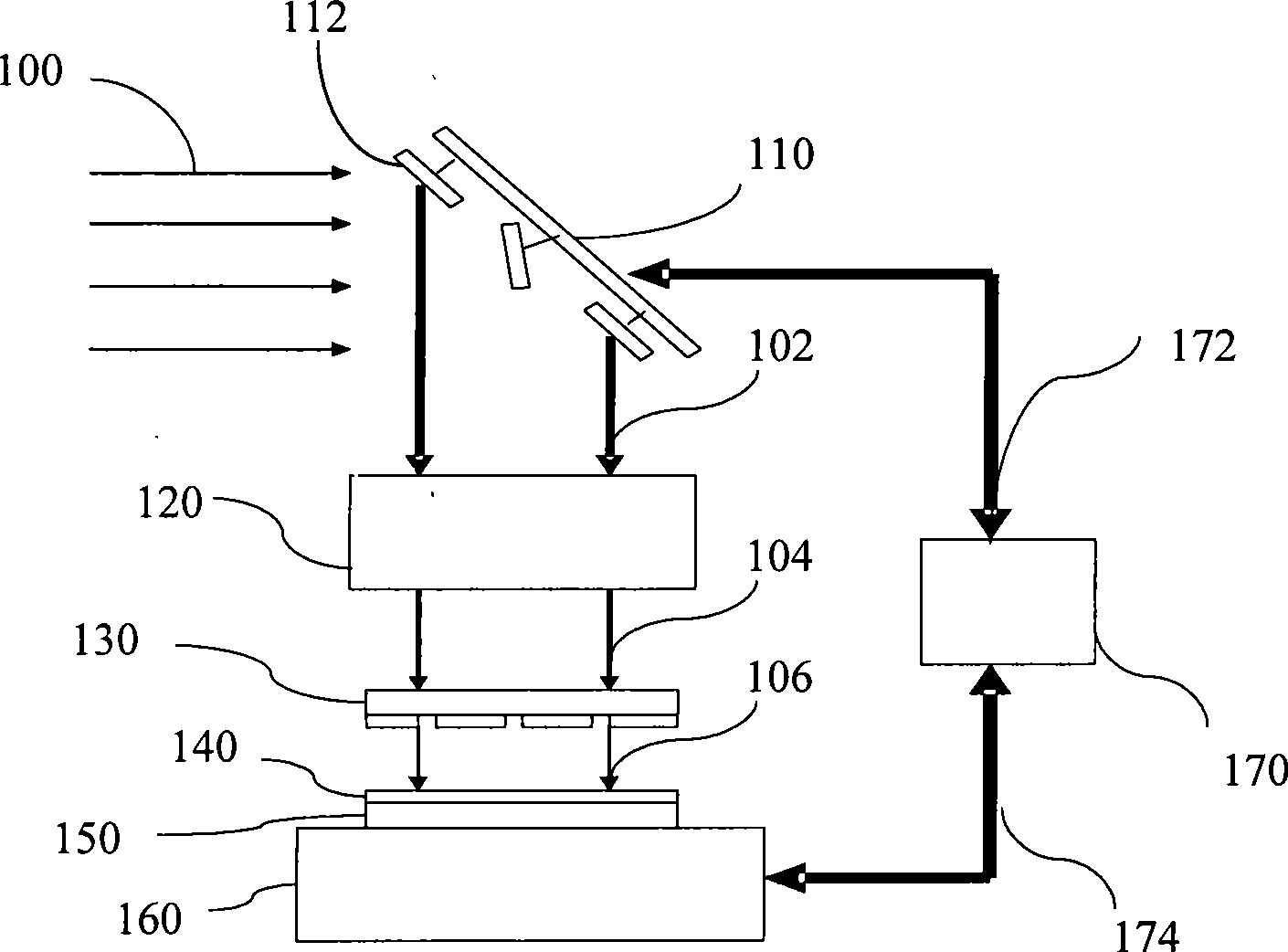
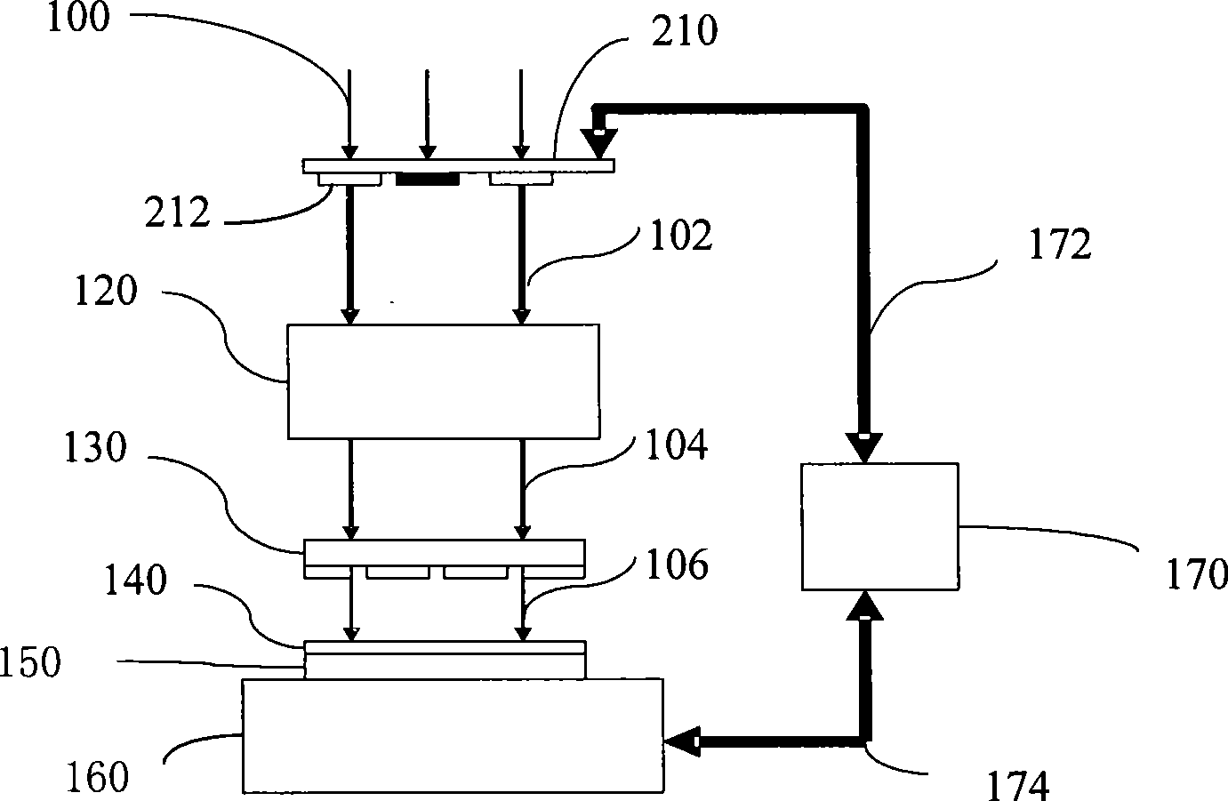
[0037] In current maskless lithography, such as zone plate array lithography, the resolution is mainly limited by the resolution of the microlenses used for focusing. For this reason, the maskless lithography system based on nanolenses proposed by the present invention adopts nanolenses to form a focusing array, and an optical imaging system provides the patterned light beam array required for exposing photoresist on a semiconductor substrate, for example, Each microbeam in the beam array corresponds to a pixel on the semiconductor substrate, and the patterned beam array will control each pixel to be bright or dark according to the exposure pattern to be generated. Each nano-lens in the focusing array corresponds to focusing each micro in the patterned light beam array to project to the semiconductor substrate. The semiconductor substrate is placed on a movable platform, for example, and during exposure, the exposure area on the semiconductor substrate can be selected by movin...


PUM

PropertyMeasurementUnit
Thicknessaaaaaaaaaa

Abstract

The invention discloses a maskless photo-etching system based on nanometer lenses, which is used to increase exposure pixel resolution of maskless photo-etching. The maskless photo-etching system comprises a movable platform, an optical imaging system and a focusing array, wherein a to-be-exposed element is placed on the movable platform, the optical imaging system provides a patterning beam array needed for exposing the element, and the focusing array is formed by nanometer lenses, wherein every nanometer lens correspondingly focuses on every beam projected to the element in the patterning beam array. The nanometer lenses can have pixel resolution which is superior to that of the traditional zone plate, and even can break through the diffraction limitation of 1 / 2 wavelength of an optical lens. Further, the work distance of the nanometer lens can range from 1micron to 100 microns.

Description

technical field [0001] The present invention relates to semiconductor manufacturing equipment, and more particularly to a maskless photolithography system using nano lenses as focusing elements. Background technique [0002] In traditional projection optical lithography, the pattern on the mask is reduced several times (usually 4-10 times) by an optical system and projected onto the photoresist. Then, a reduced mask pattern can be obtained on the photoresist through development. [0003] With the development of semiconductor technology, the feature size of integrated circuits (Integrated Circuits, IC for short) is shrinking day by day, and traditional photolithography is facing more and more challenges, one of which is the cost and manufacturing time of masks. A set of masks for 90nm integrated circuits costs as much as $1 million, and the manufacturing cycle is as long as 3 months, and 70% of them may not be usable. For low-volume IC production, such as custom integrated ...

Claims


Application Information

Patent Timeline
IPC IPC(8): G03F7/00G03F7/20G02B3/00
Inventor 阮巍
Owner 上海科学院
Why Eureka
Try Eureka