
Flat suction nozzle and chip fetching/laying machine as well as semiconductor test method thereof
A semiconductor, flat technology, used in semiconductor chip pick and place nozzles and chip pick and place machines and their testing fields to reduce scratches
- Summary
- Abstract
- Description
- Claims
- Application Information
AI Technical Summary
Problems solved by technology
Method used
Image

Examples
Embodiment Construction
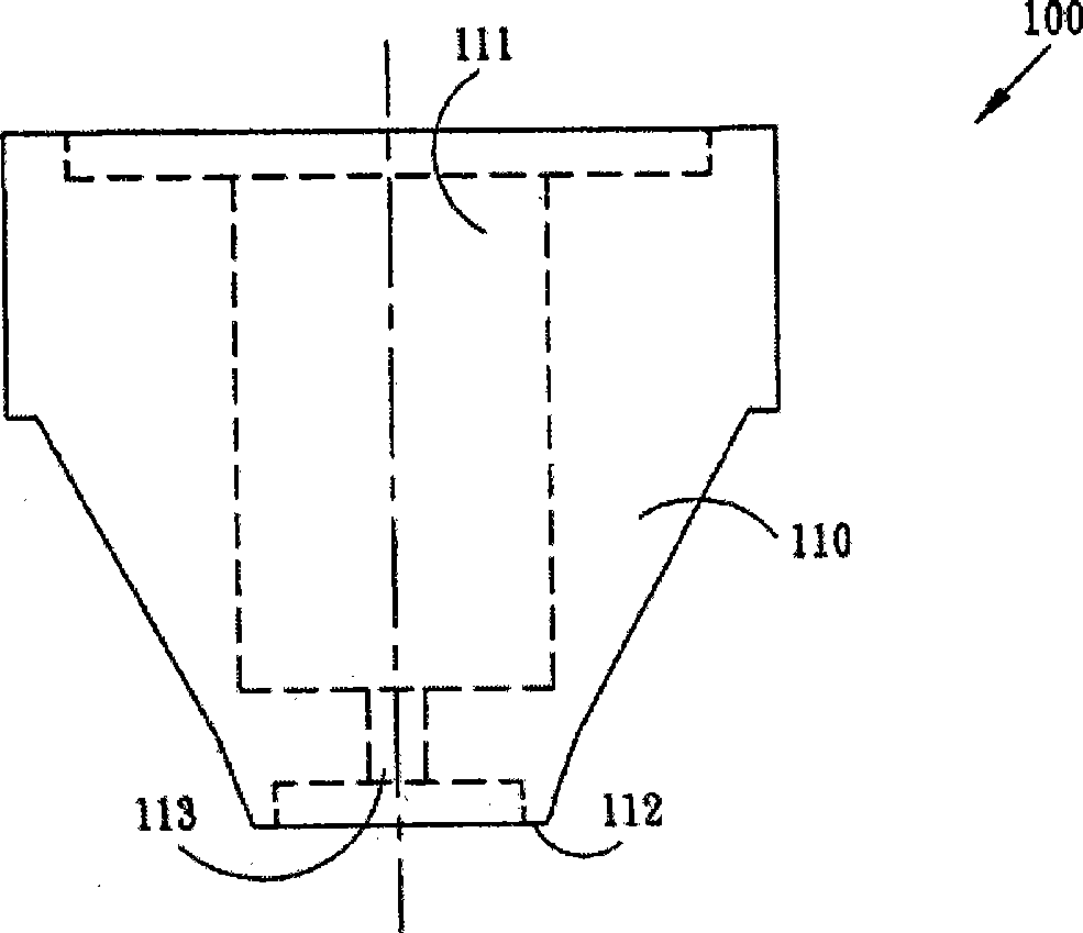
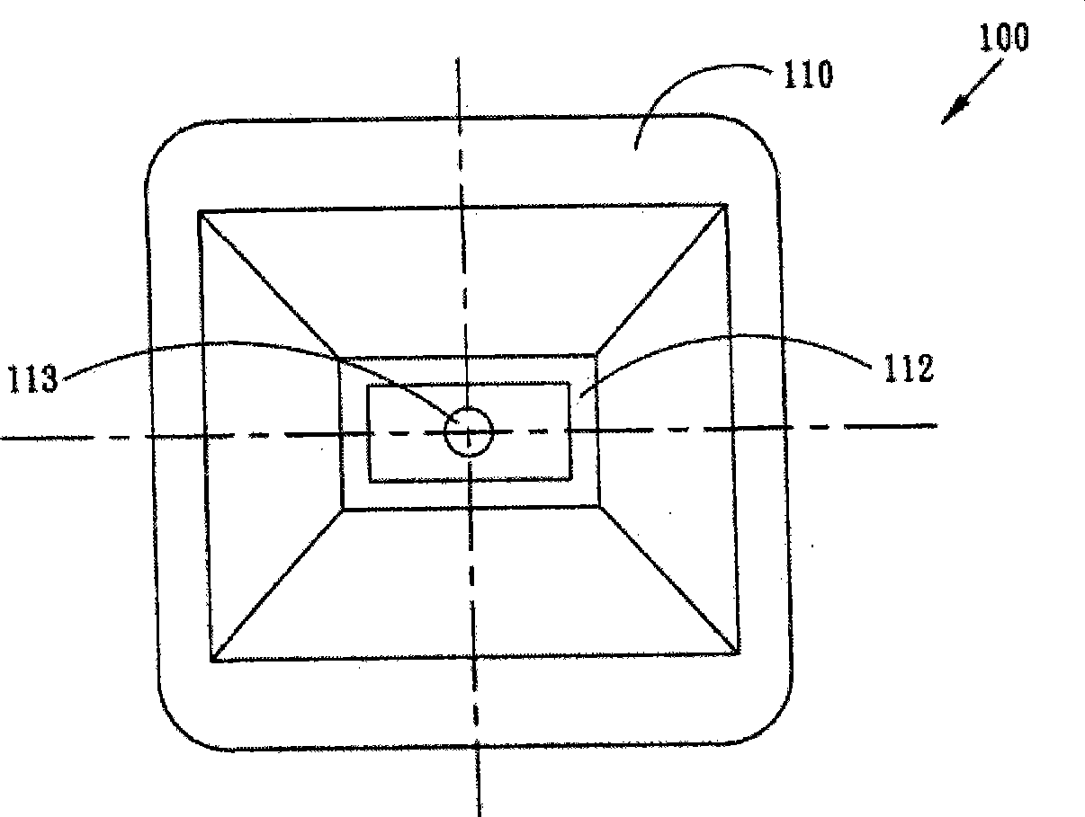
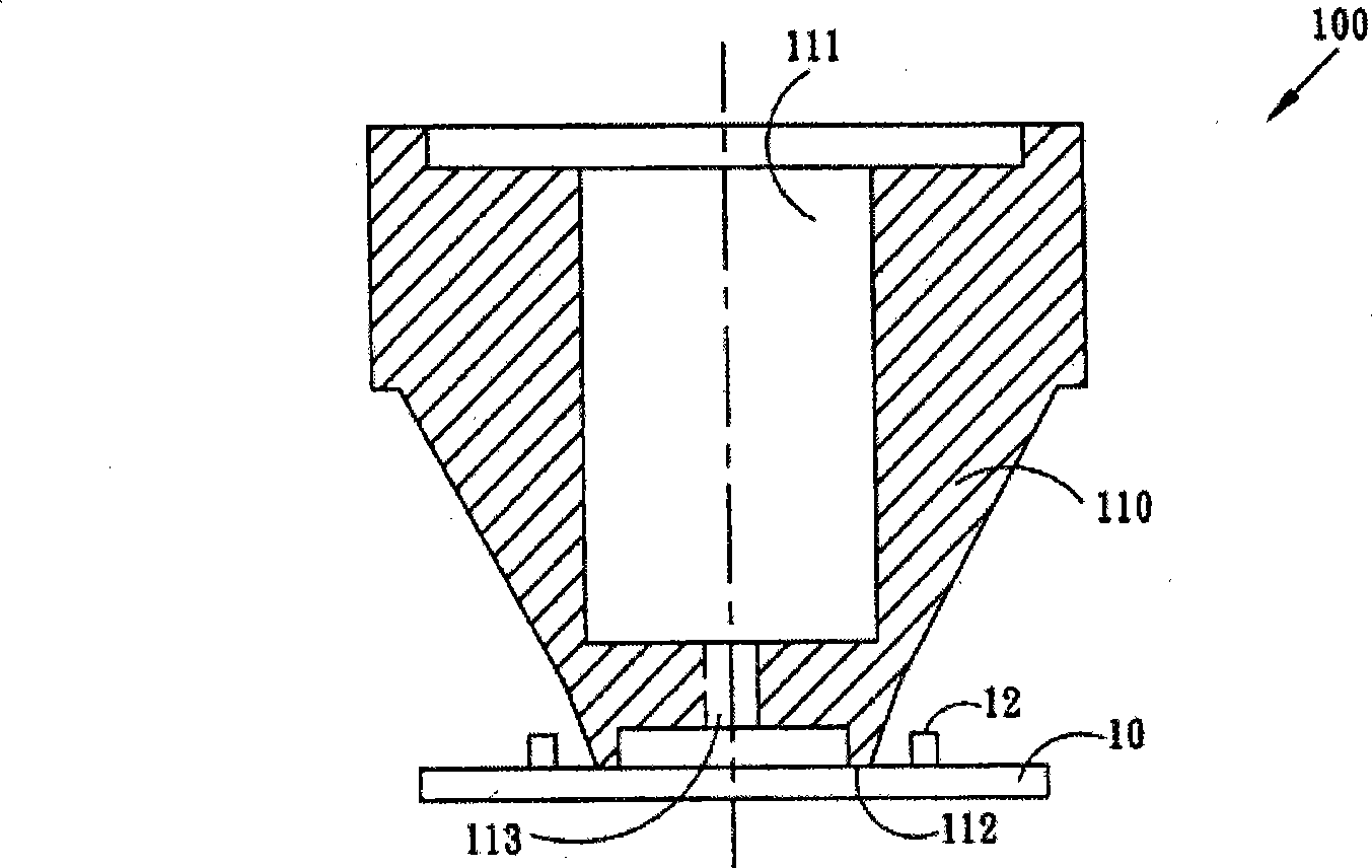
[0042] In order to further illustrate the technical means and effects that the present invention adopts to achieve the intended invention purpose, below in conjunction with the accompanying drawings and preferred embodiments, the flat suction nozzle, the chip pick-and-place machine and the semiconductor testing method thereof proposed according to the present invention will be described. The specific embodiment, structure, test method, steps, features and effects thereof are described in detail below.
[0043] The aforementioned and other technical contents, features and effects of the present invention will be clearly presented in the following detailed description of preferred embodiments with reference to the drawings. Through the description of the specific implementation mode, when the technical means and functions adopted by the present invention to achieve the predetermined purpose can be obtained a deeper and more specific understanding, but the accompanying drawings ar...
PUM
| Property | Measurement | Unit |
|---|---|---|
| Shore hardness | aaaaa | aaaaa |
Abstract
Description
Claims
Application Information