Image sensor and method for manufacturing the sensor

An image sensor and pattern technology, applied in semiconductor/solid-state device manufacturing, electrical solid-state devices, semiconductor devices, etc., to reduce noise and image delay

Inactive Publication Date: 2009-07-01
DONGBU HITEK CO LTD
View PDF0 Cites 17 Cited by
  • Summary
  • Abstract
  • Description
  • Claims
  • Application Information

AI Technical Summary

Problems solved by technology

Noise or image lag (lag) can occur if charge flows back toward the photodiode

Method used


Image

  • Image sensor and method for manufacturing the sensor
  • Image sensor and method for manufacturing the sensor
  • Image sensor and method for manufacturing the sensor

Examples


Embodiment Construction

[0015] The words "on" or "over" or "on" are used in the following description, those skilled in the art should understand that when referring to When a layer, region, pattern or structure is present, the layer, region, pattern or structure may be directly on another layer or structure, or intervening layers, regions, patterns or structures may also be present. When the words "under" or "beneath" are used in the following description, those skilled in the art will understand that when referring to a layer, region, pattern or structure, Such layers, regions, patterns or structures may be directly underlying other layers or structures, or intervening layers, regions, patterns or structures may also be present.

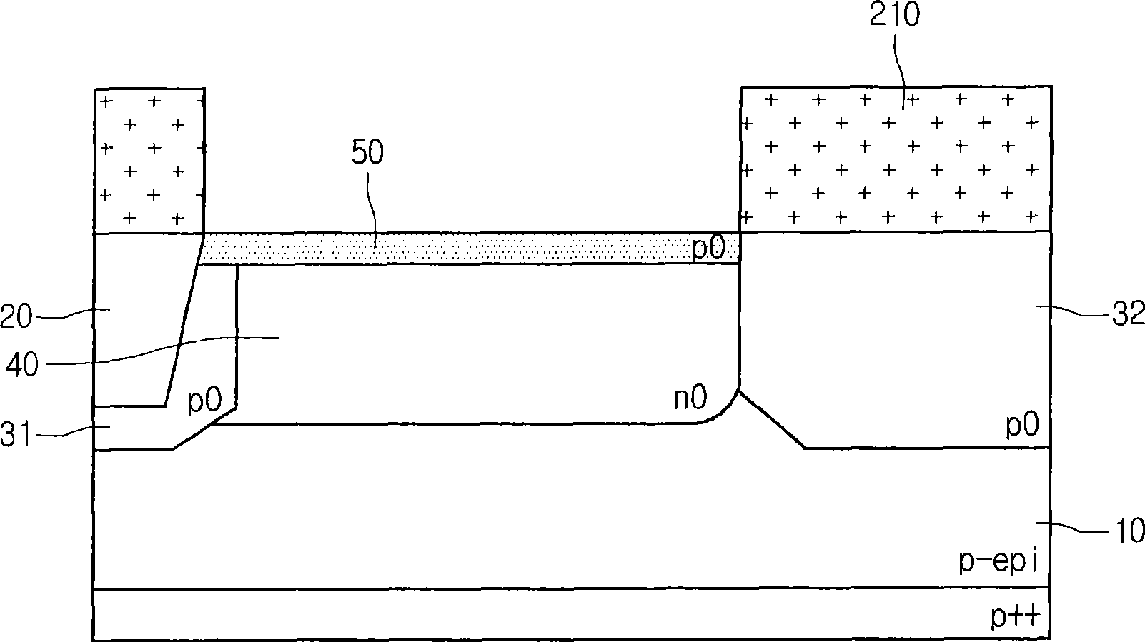
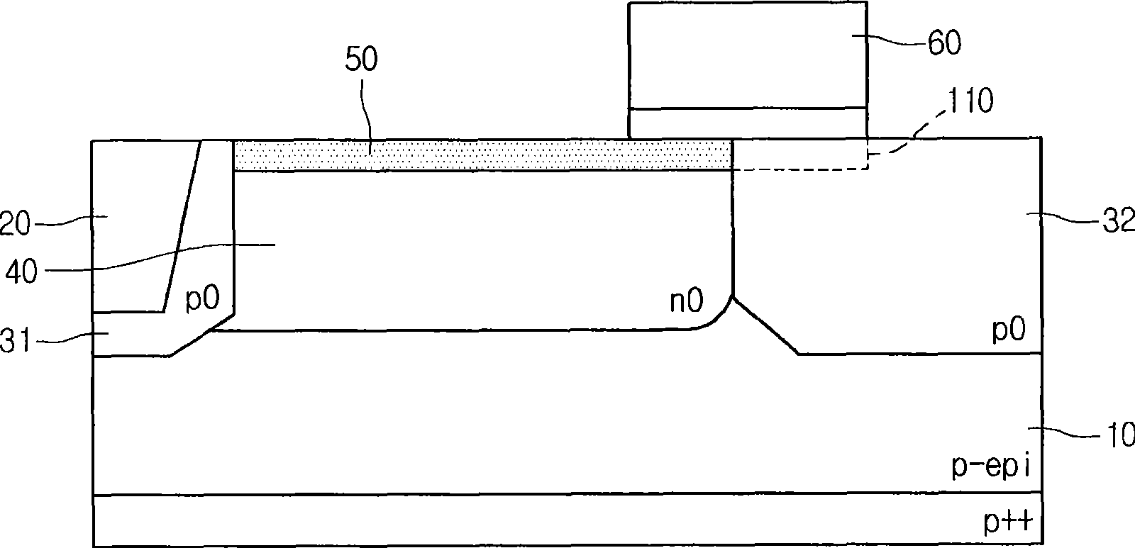
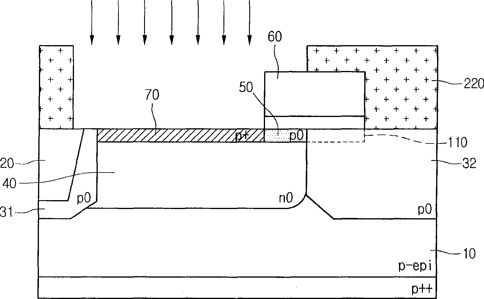
[0016] Figure 5 is a cross-sectional view showing an image sensor according to an embodiment of the present invention.

[0017] see Figure 5 , the image sensor includes: a gate 60 located on a semiconductor substrate 10; a first p-type doped region 50 and a second p-...


PUM


Abstract

An image sensor and manufacturing method thereof are provided. The image sensor can include a gate on a semiconductor substrate, first and second p-type doping areas below the gate, a third p-type doping area adjacent to the first p-type doping area, and a fourth p-type doping area adjacent to the third p-type doping area. An n-type doping area can be provided in the semiconductor substrate such that at least a portion of the n-type doping area is disposed below the first, third, and fourth p-type doping areas. A floating diffusion area can be provided adjacent to the second p-type doping area. The invention can prevent the electrons of the channel area from flowing back toward the photodiode, so that noise and image lagging can be reduced.

Description

technical field [0001] The present invention relates to an image sensor and a manufacturing method thereof, and more particularly, to an image sensor capable of improving electron transfer efficiency by adjusting the doping concentration of a channel region. Background technique [0002] Image sensors are semiconductor devices that convert optical images into electrical signals. Image sensors may be classified into Charge Coupled Device (CCD) image sensors or Complementary Metal Oxide Semiconductor (CMOS) image sensors. [0003] Generally, a CMOS image sensor provides metal-oxide-semiconductor (MOS) transistors corresponding to the number of pixels through CMOS technology and uses peripheral devices such as control circuits and signal processing circuits to sequentially detect outputs in a switching manner. [0004] In addition, a CMOS image sensor generally includes a photodiode for receiving light to generate photocharges and MOS transistors arranged according to unit pix...

Claims


Application Information

Patent Timeline
Patent Type & Authority Applications(China)
IPC IPC(8): H01L27/146H01L21/822
CPCH01L27/14603H01L27/14689H01L27/146
Inventor 金钟玟
Owner DONGBU HITEK CO LTD
Why Eureka
Try Eureka