Cu-Mn alloy sputtering target and semiconductor wiring

A technology for sputtering targets and semiconductors, which is applied in semiconductor devices, semiconductor/solid-state device manufacturing, semiconductor/solid-state device components, etc., can solve problems such as unclear mutual relations, contamination of Si substrates, and unreliable barrier films, etc., to achieve improved Anti-electromigration (EM), simplification of film formation process, and effects of pollution prevention

Active Publication Date: 2009-07-01
JX NIPPON MINING & METALS CORP
View PDF20 Cites 24 Cited by
  • Summary
  • Abstract
  • Description
  • Claims
  • Application Information

AI Technical Summary

Problems solved by technology

[0004] Copper or copper alloys are very effective as wiring materials for semiconductors, but the following problems arise: Copper itself is a very active metal, so it diffuses easily, and contaminates the Si substrate or its surroundings through the semiconductor Si substrate or the insulating film on it.
Therefore, there is a problem that it cannot be called a sufficient barrier film because Cu and additive elements are in a state where intermetallic compounds are not formed.
However, these are all limited to the control of the crystal orientation, and do not have the purpose of preventing contamination around the wiring due to Cu diffusion. In addition, the relationship between the composition of the copper alloy target used to form the barrier film and the crystal orientation is not good. clear

Method used


Image

  • Cu-Mn alloy sputtering target and semiconductor wiring
  • Cu-Mn alloy sputtering target and semiconductor wiring
  • Cu-Mn alloy sputtering target and semiconductor wiring

Examples


Embodiment 1~6

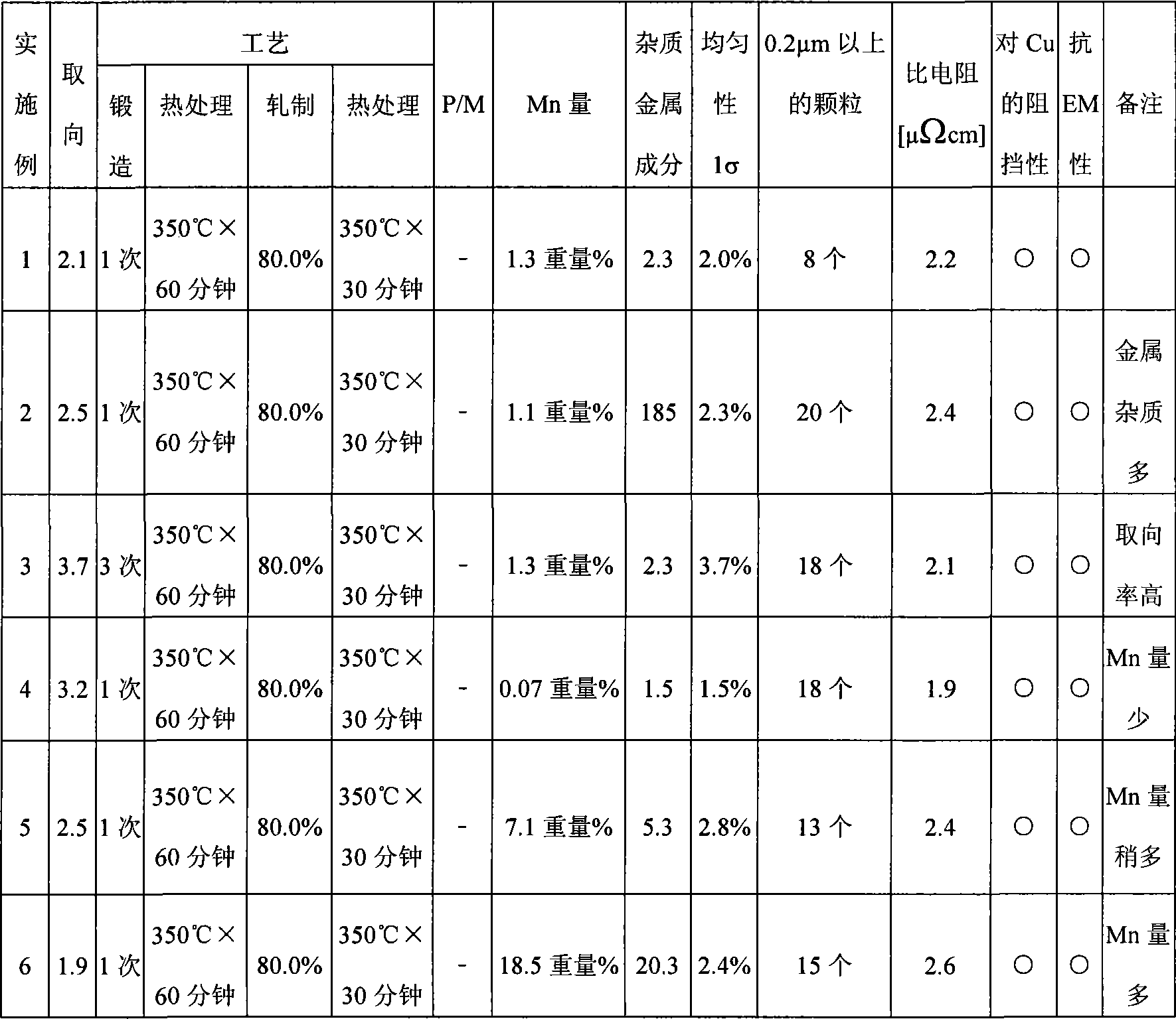
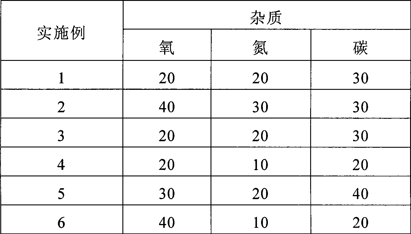
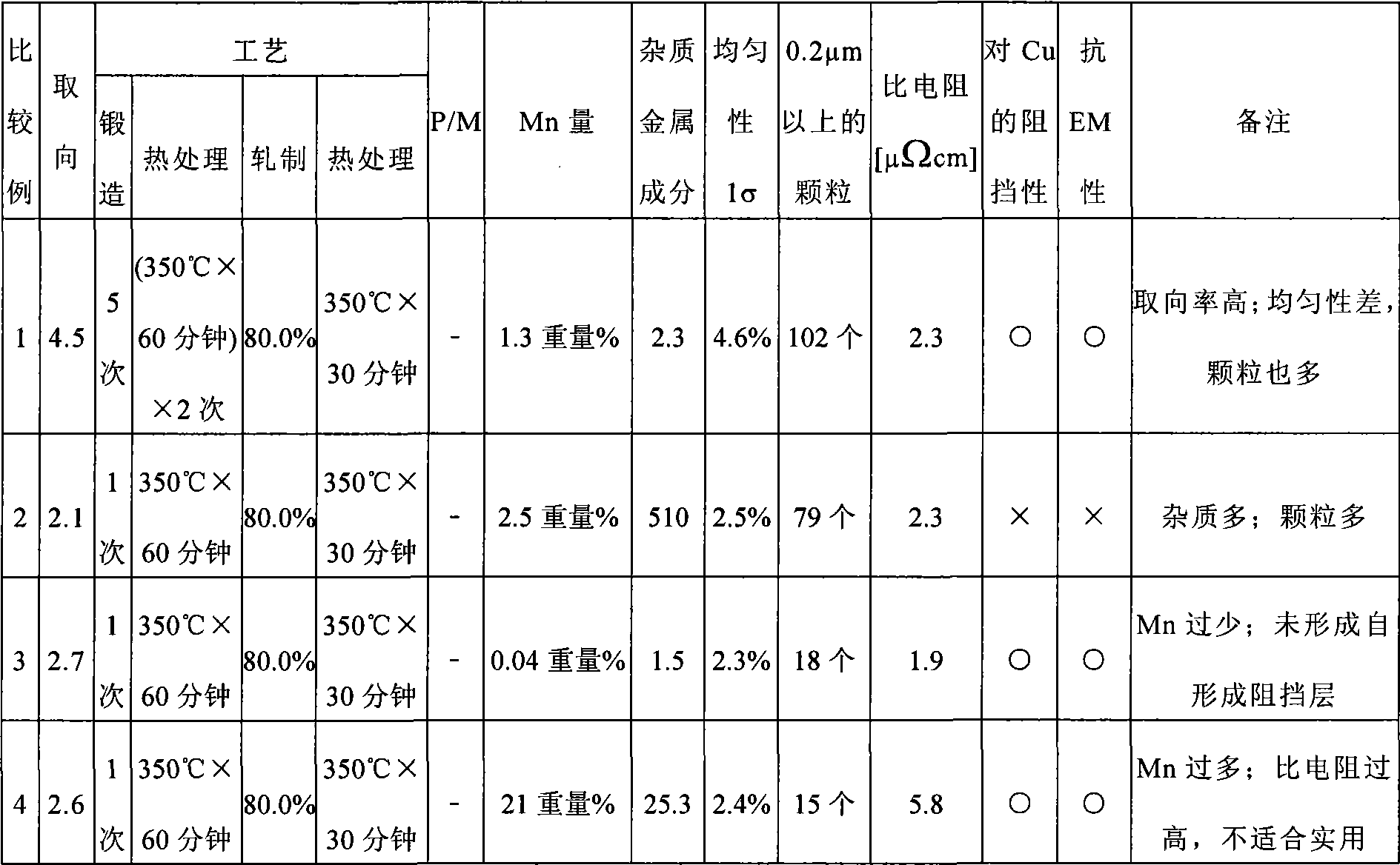
[0078] Prepare high-purity copper (Cu) with a purity of 6N or higher and manganese (Mn) with a level of 5N, and use a high-purity graphite crucible to melt in a high-vacuum atmosphere to obtain a high-purity alloy. Table 1 shows the alloy compositions of Examples 1 to 6 produced.

[0079] The alloyed molten metal is cast into a water-cooled copper mold under a high vacuum atmosphere to obtain an ingot. Next, after removing the surface layer of the produced ingot and making it into φ85×100h, it was heated to 350°C, and then directly hot forged (first forging) into φ105×65h, and then hot rolled in the next step. Among them, the following operations are only performed on Example 3: hot forging (first forging) to φ105×65h, then reheating to 350°C, radial forging (second forging) to φ85×100h, and further Its hot heading forging (the third forging) is φ105×65h. The number of times of forging is arbitrary. Next, hot rolling was performed at 400° C. to φ200×18 t, and further cold r...

Embodiment 1

[0090] (Film characteristics and evaluation of Example 1)

[0091] Example 1 contained 1.3% by weight of Mn, and the total amount of Be, B, Mg, Al, Si, Ca, Ba, La, and Ce was 2.3 ppm by weight. The manufacturing conditions of the target are shown in Table 1. The results are shown in Table 1. When the copper alloy wiring and seed layer for semiconductors are made, the Cu diffusion resistance (barrier property) is excellent, and all show good anti-EM characteristics (almost no disconnection) and film Resistance (low resistance: 2.2 μΩcm). This is because manganese diffuses to the upper part, the side surface, and the lower part of the wiring to form a good barrier film, and at the same time, the resistance of the central part of the wiring is lowered. In addition, almost no disconnection was observed, which is considered to be because the total amount of Be, B, Mg, Al, Si, Ca, Ba, La, and Ce was reduced to 2.3 wtppm.

[0092] In this Example 1, as the structure of the Cu-Mn a...

Embodiment 2

[0096] (Film characteristics and evaluation of Example 2)

[0097] Example 2 contained 1.1% by weight of Mn, and the total amount of Be, B, Mg, Al, Si, Ca, Ba, La, and Ce was 185 ppm by weight. The manufacturing conditions of the target are shown in Table 1. The results are shown in Table 1. When the copper alloy wiring and seed layer for semiconductors are made, the Cu diffusion resistance (barrier property) is excellent, and all show good anti-EM characteristics (almost no disconnection) and film Resistance (low resistance: 2.4 μΩcm). This is because manganese diffuses to the upper part, the side surface, and the lower part of the wiring to form a good barrier film, and at the same time, the resistance of the central part of the wiring is lowered. In addition, almost no disconnection is observed, which is considered to be because the total amount of Be, B, Mg, Al, Si, Ca, Ba, La, and Ce is 185 ppm by weight, which is within the condition range of the present invention. Ho...


PUM


Abstract

This invention provides a Cu-Mn alloy sputtering target characterized by comprising 0.05 to 20% by weight of Mn and not more than 500 ppm by weight in total of Be, B, Mg, Al, Si, Ca, Ba, La, and Ce with the balance consisting of Cu and unavoidable impurities. There is also provided a copper alloy wiring for a semiconductor, wherein a self-diffusion suppression function can be imparted to the copper alloy wiring for a semiconductor per se to effectively prevent contamination of a part around the wiring by the diffusion of active Cu. Further, in the copper alloy wiring for a semiconductor, for example, electromigration (EM) resistance and corrosion resistance have been improved, a barrier layer can be arbitrarily and easily formed, and, further, the film forming step of a copper alloy wiring for a semiconductor can be simplified. A sputtering target for the formation of the wiring, and a method for forming a copper alloy wiring for a semiconductor are also provided.

Description

technical field [0001] The present invention relates to a sputtering target for copper alloy wiring for semiconductors that can effectively prevent contamination around the wiring caused by the diffusion of active Cu, and in particular to a Cu- Mn alloy sputtering targets and copper alloy wiring for semiconductors. Background technique [0002] Conventionally, Al alloys (specific resistance about 3.0 μΩ·cm) have been used as wiring materials for semiconductor devices, but copper wiring with lower resistance (specific resistance about 1.7 μΩ·cm) has gradually been used as wiring becomes smaller. The current copper wiring formation process is generally carried out as follows: After forming a diffusion barrier layer such as Ta or TaN in the concave portion of the contact hole or the wiring groove, copper or copper alloy is sputtered to form a film. [0003] Generally, electrolytic copper with a purity of about 4N (excluding gas components) is used as a crude metal, and high-pu...

Claims


Application Information

Patent Timeline
Patent Type & Authority Applications(China)
IPC IPC(8): C23C14/34H01L21/3205H01L21/285H01L23/52
CPCC23C14/3414H01L23/53233H01L2924/0002H01L2924/00C22C9/05C23C14/34H01L21/285H01L21/3205
Inventor 入间田修一宫田千荣
Owner JX NIPPON MINING & METALS CORP
Why Eureka
Try Eureka