
Sputtering target and manufacturing method therefor

A manufacturing method and sputtering target technology, which are applied in sputtering coating, semiconductor/solid-state device manufacturing, ion implantation plating, etc., to achieve the effects of excellent corrosion resistance, pollution prevention, and deformation suppression

Active Publication Date: 2014-05-28
JX NIPPON MINING & METALS CORP
View PDF7 Cites 4 Cited by
  • Summary
  • Abstract
  • Description
  • Claims
  • Application Information

AI Technical Summary

Problems solved by technology

However, this technology softens the melted portion by laser irradiation so that the hardness of the bottom surface of the pit is lower than the hardness of the surface of the non-eroded portion, and it is not a technology to increase the strength of the target to control target deformation during sputtering.

Method used


Image

  • Sputtering target and manufacturing method therefor

Examples


Embodiment 1

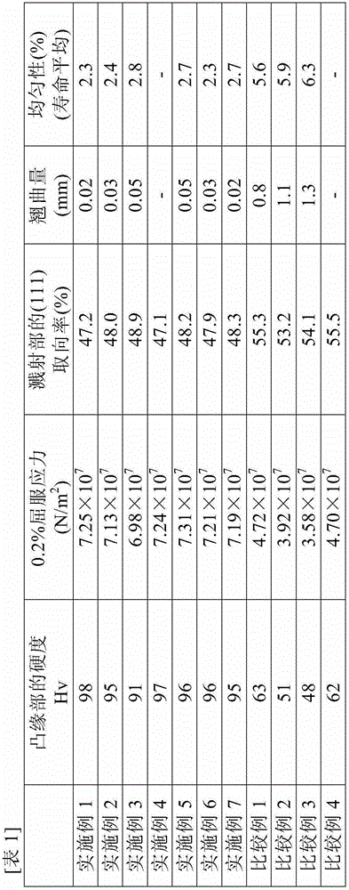
[0039] In Example 1, the Cu-Mn alloy (Mn1wt%) ingot obtained by melting and casting was forged and rolled to produce a rolled plate, and the outer peripheral portion (corresponding to the flange portion) of the rolled plate was further forging. Next, heat treatment is performed on this, and then quenched to obtain a target raw material. Then, a backing plate-integrated sputtering target with a diameter of 540 mm and a thickness of 25 mm was produced by machining. The physical properties of this target were evaluated. As a result, the Vickers hardness Hv of the flange was 98, and the 0.2% yield stress of the flange was 7.25×10 7 N / m 2 , the (111) orientation rate of the sputtered surface is 47.2%.

Embodiment 2

[0041] In Example 2, the Cu-Mn alloy (Mn1wt%) ingot obtained by melting and casting was forged and rolled to produce a rolled plate, and the outer peripheral portion (corresponding to the flange portion) of the rolled plate was further processed. forging. Next, heat treatment is performed on this, and then quenched to obtain a target raw material. Then, a backing plate-integrated sputtering target with a diameter of 540 mm and a thickness of 25 mm was produced by machining. The physical properties of this target were evaluated. As a result, the Vickers hardness Hv of the flange was 95, and the 0.2% yield stress of the flange was 7.13×10 7 N / m 2 , the (111) orientation rate of the sputtered surface is 48.0%.

Embodiment 3

[0043] In Example 3, the Cu-Mn alloy (Mn1wt%) ingot obtained by melting and casting was forged and rolled to produce a rolled plate, and the outer peripheral portion (corresponding to the flange portion) of the rolled plate was further forging. Next, heat treatment is performed on this, and then quenched to obtain a target raw material. Then, a backing plate-integrated sputtering target with a diameter of 540 mm and a thickness of 25 mm was produced by machining. The physical properties of this target were evaluated. As a result, the Vickers hardness Hv of the flange was 91, and the 0.2% yield stress of the flange was 6.98×10 7 N / m 2 , the (111) orientation rate of the sputtered surface is 48.9%.


PUM

PropertyMeasurementUnit
electrical resistivityaaaaaaaaaa
orientation degreeaaaaaaaaaa

Abstract

A sputtering target with an integrated backing plate characterized in that the Vickers hardness (Hv) of a flange part is at least 90, and the 0.2% yield stress of the flange part is at least 6.98x10<7> N / m2. By increasing the mechanical strength of only the flange part of the target, deformation of the target during sputtering can be suppressed and, furthermore, a highly uniform thin film, with none of the variable sputtering characteristics of the prior art, can be made. As a result, it is possible to increase the reliability and yield of semiconductor products, the miniaturization and high-integration of which are continually advancing.

Description

technical field [0001] The present invention relates to a sputtering target for forming a thin film of a semiconductor device. In particular, it relates to a copper-manganese alloy sputtering target having a function of suppressing self-diffusion for forming semiconductor copper alloy wiring. Background technique [0002] Conventionally, Al alloys (resistivity: about 3.0 μΩ·cm) have been used as wiring materials for semiconductor elements, but copper wiring (resistivity: about 2.0 μΩ·cm) with lower resistance has been put into practical use as wiring becomes smaller. change. As a process for forming copper wiring, a process of forming a diffusion barrier layer such as Ta or TaN on a wiring or a wiring groove and then sputtering copper into a film is generally performed. Copper is usually used as a sputtering target by using electrolytic copper with a purity of about 4N (excluding gas components) as a crude metal, and using a wet or dry high-purification process to produce ...

Claims


Application Information

Patent Timeline
Patent Type & Authority Applications(China)
IPC IPC(8): C23C14/34H01L21/28H01L21/285
CPCC23C14/34C23C14/3414H01L21/285H01J37/3435C23C14/3407H01J37/3414C22C9/05H01J37/3426B21D53/00
Inventor 长田健一大月富男冈部岳夫牧野修仁福岛笃志
Owner JX NIPPON MINING & METALS CORP
Learn More