

Method for preparing organic semiconductor material rubrene micro-nano wire
An organic semiconductor and rubrene technology, which is applied in semiconductor devices, semiconductor/solid-state device manufacturing, metal material coating technology, etc., can solve the problems of complex preparation process and difficult precise control of finished product size, and achieve the goal of simplifying the preparation process Effect
Inactive Publication Date: 2010-12-22
SUZHOU INST OF NANO TECH & NANO BIONICS CHINESE ACEDEMY OF SCI
View PDF0 Cites 0 Cited by
- Summary
- Abstract
- Description
- Claims
- Application Information
AI Technical Summary
Problems solved by technology
[0004] The present invention aims to provide a method for preparing rubrene micro-nanowires, an organic semiconductor material, which overcomes the problems that the existing preparation process is too complicated and the size of the finished product is difficult to accurately control
Method used
View moreImage
Smart ImageViewing Examples

Examples
Embodiment 1
[0030] Example 2
Embodiment 2
[0032] Example 3
Embodiment 3
[0034] Example 4
Login to View More PUM
| Property | Measurement | Unit |
|---|---|---|
| diameter | aaaaa | aaaaa |
| diameter | aaaaa | aaaaa |
| height | aaaaa | aaaaa |
Abstract
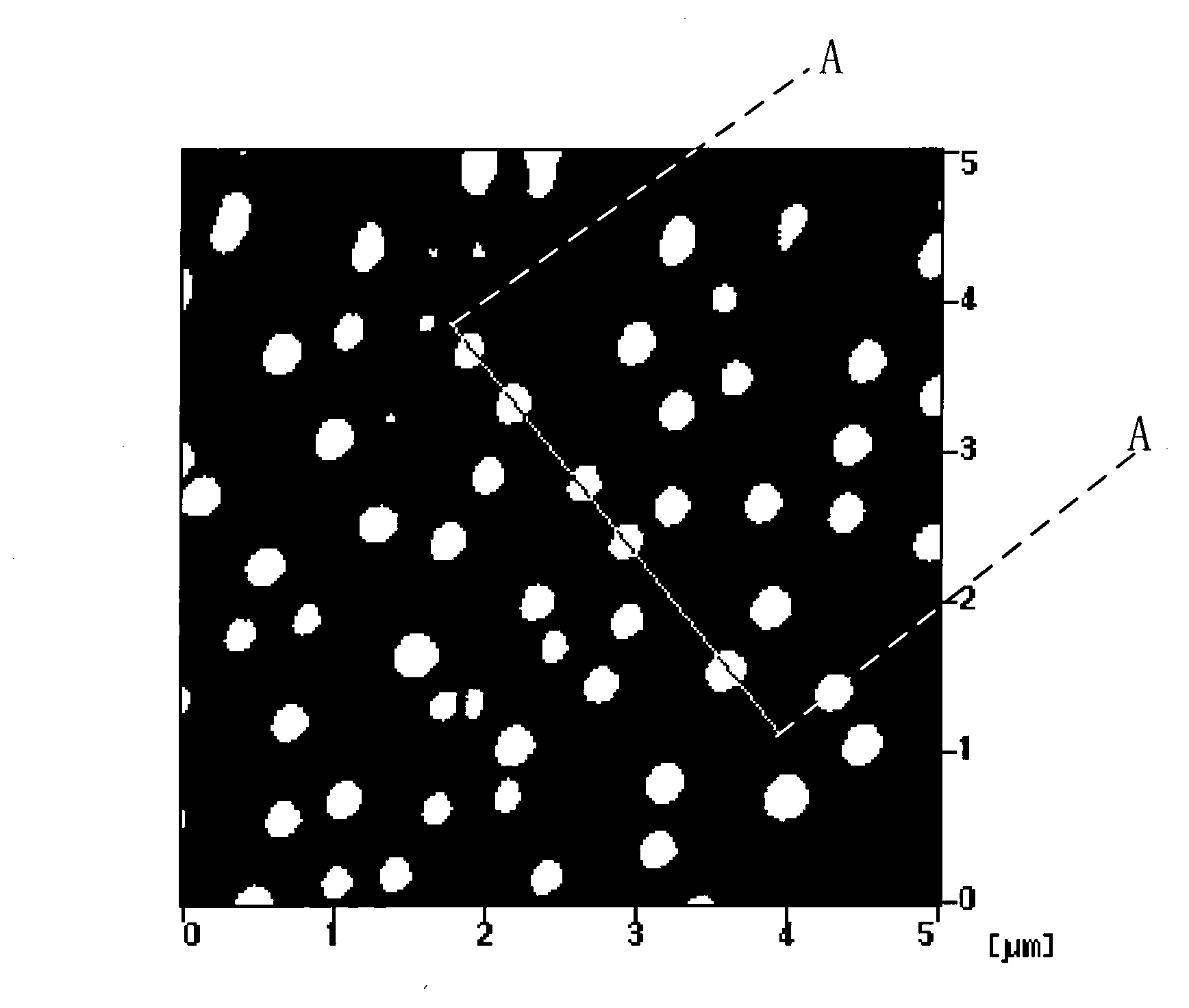
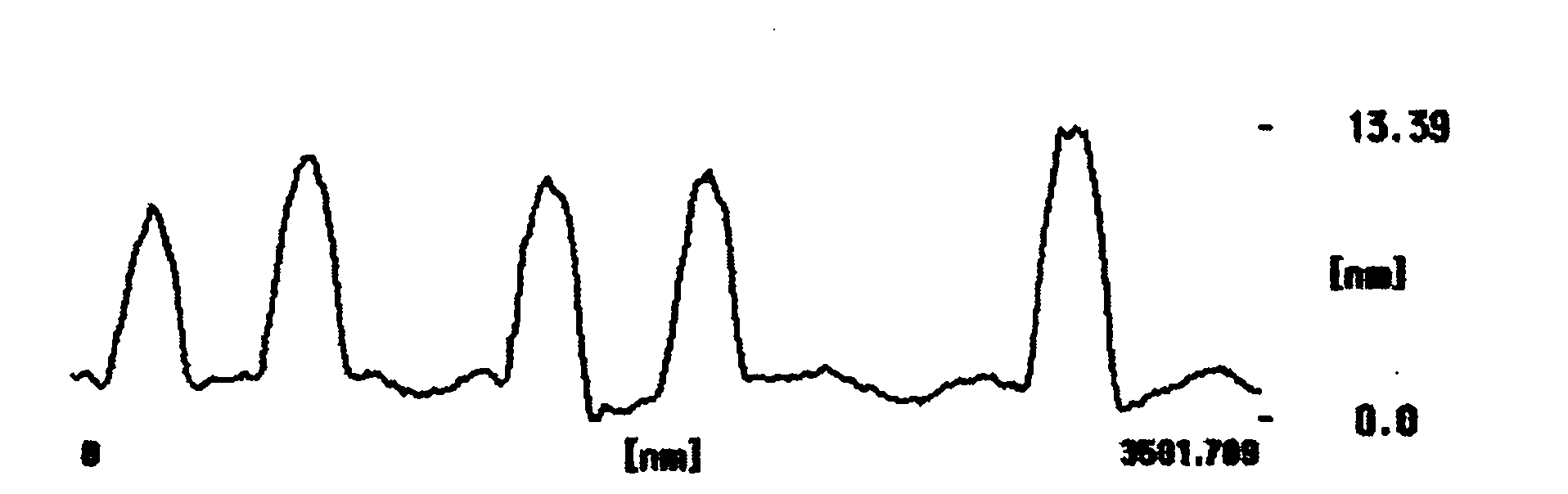
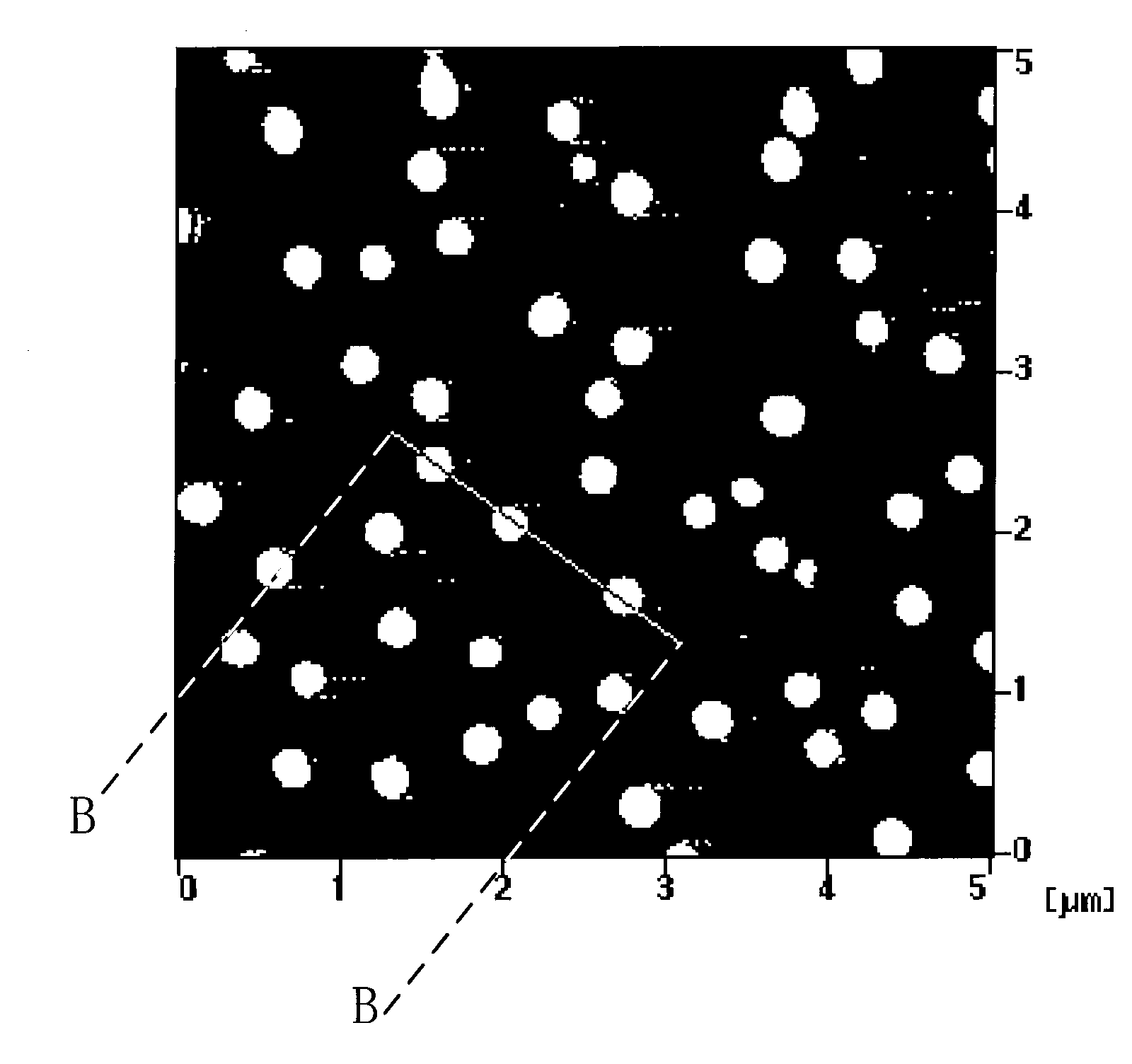
The invention discloses method of preparing rubrene micro-nanowire of organic semiconductor materials, and the method is characterized by using rubrene as a raw material for vapor deposition, using naphthacene single crystal growing through clean slices of silicon or physics gas-phase transmission method as the substrate, adopting a vacuum vapor deposition method, and under a condition of controlling the deposition rate and the deposition time, forming rubrene micro-nanowire with a standard size through deposition on the substrate of the semiconductor.According to the invention, because of adopting a vacuum vapor deposition method capable of controlling the deposition rate and deposition time accurately, the size of the rubrene micro-nanowire can be controlled accurately and simultaneously the preparation technique can also be simplified.
Description
technical field [0001] The invention relates to an organic semiconductor material rubrene, in particular to a controllable preparation method of the organic semiconductor material rubrene micro-nano wire. Background technique [0002] The rubrene material is an organic semiconductor that has been studied and applied more in recent years. In addition to its application in organic transistors, it has also played an unexpected and outstanding effect in OLEDs and solar cells. Since 2004, Sundar et al published the research results of rubrene single crystal transistors in the journal "Science" and showed that rubrene has the highest mobility in all organic materials (V.C.Sundar, et al, Science, 2004 , 303:1644), rubrene materials have received widespread attention, and more and more intelligent minds have begun to invest in research in this area. [0003] In 2006, Zhenan Bao et al. of Stanford University in the United States prepared rubrene micro-nano materials by combining phy...
Claims
Login to View More Application Information
Patent Timeline
 Patent Type & AuthorityPatents(China)
IPC IPC(8): C23C14/06C23C14/04C23C14/26H01L51/00H10K99/00
Inventor曾雄辉徐科张锦平张露黄凯
OwnerSUZHOU INST OF NANO TECH & NANO BIONICS CHINESE ACEDEMY OF SCI