Method for manufacturing microlens and method for manufacturing solid-state image sensor

A manufacturing method and technology of microlens, applied in the direction of lens, semiconductor/solid-state device manufacturing, instruments, etc., can solve the problems of reducing sensitivity, reducing design freedom, increasing, etc., to improve convergence characteristics, reduce costs and reduce costs Effect

Inactive Publication Date: 2013-03-13
SONY CORP
View PDF2 Cites 0 Cited by
  • Summary
  • Abstract
  • Description
  • Claims
  • Application Information

AI Technical Summary

Problems solved by technology

However, since the resist lens pattern of the convex lens shape that determines the shape of the microlens is determined by the mobility of the resist, the degree of freedom in design is reduced, and it is difficult to obtain desired light diffusion characteristics in the pixel
[0015] In addition, when resist patterns are softened and liquefied by heating, there arises a problem that if adjacent resist patterns are in contact with each other, the resist patterns are smoothly connected together due to surface tension, thereby making the lens shape deformation
Therefore, there arises a problem that the angle at which light is incident to the microlens array increases in the peripheral area of ​​the solid-state image sensor, resulting in a large deviation from the light-receiving effective area and a decrease in sensitivity due to a decrease in the light-receiving rate.
[0019] The former method has the problem of using a large device for electron beam exposure, while the latter method has the problems of low degree of freedom for forming a microlens having a desired shape and being difficult to apply to the miniaturization of the microlens

Method used


Image

  • Method for manufacturing microlens and method for manufacturing solid-state image sensor
  • Method for manufacturing microlens and method for manufacturing solid-state image sensor
  • Method for manufacturing microlens and method for manufacturing solid-state image sensor

Examples


Embodiment Construction

[0053] A method of manufacturing a microlens according to an embodiment of the present invention is described below.

[0054] In the method of manufacturing a microlens according to an embodiment of the present invention, a microlens mold in which a reverse shape of a microlens has been formed is pressed on a microlens forming film formed on a substrate to convert the reverse shape of the microlens into onto the microlens-forming film to form microlenses.

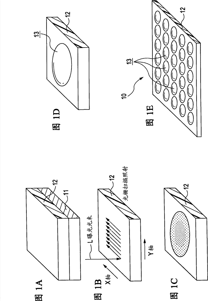
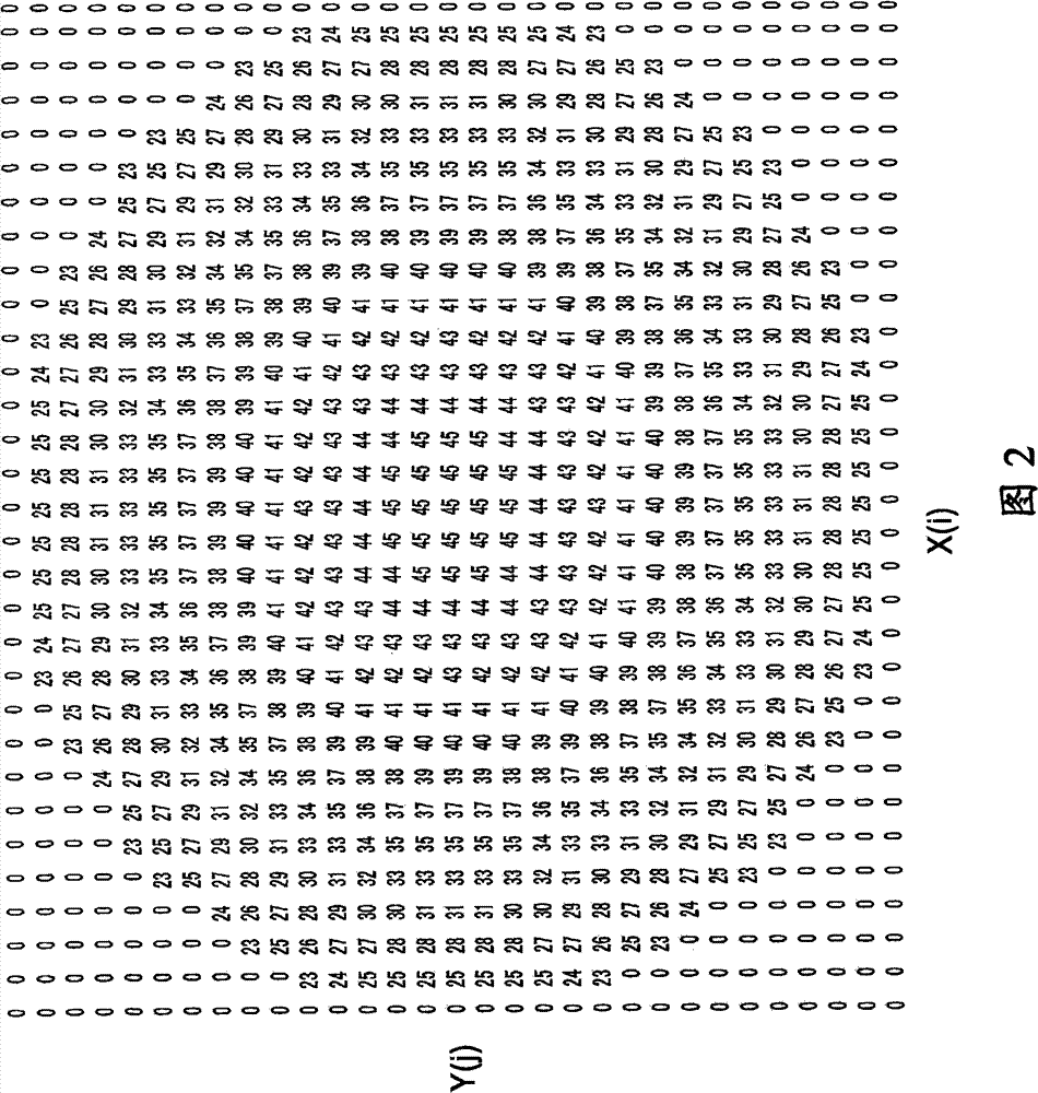
[0055] A process for forming a microlens mold is described with reference to FIGS. 1A to 1E and the process diagram of FIG. 2 .

[0056] As shown in FIG. 1A , an inorganic resist film 12 is formed on a mold substrate 11 . As the mold substrate 11, silicon dioxide (SiO 2 ) substrate or glass substrate. For the inorganic resist film 12, for example, a transition metal oxide is used. For example, tungsten oxide, molybdenum oxide, oxide of tungsten-molybdenum alloy, etc. are used. Such a material is formed on the substrate...


PUM


Abstract

A method for manufacturing a microlens includes forming a microlens by pressing a microlens mold having a reverse shape of a microlens formed therein on a microlens-forming film formed on a substrate to transfer the reverse shape of the microlens to the microlens-forming film. The microlens mold is formed by irradiating an inorganic resist film which is formed on a mold substrate with exposure light by relative two-dimensional scanning, and etching an exposed region of the inorganic resist film to form the reverse shape of the microlens. The irradiation intensity of the exposure light is adjusted to correspond to the depth of the reverse shape of the microlens from the surface of the inorganic resist film on the basis of profile data of the reverse shape of the microlens.

Description

[0001] Cross References to Related Applications [0002] The present invention contains subject matter of Japanese Patent Application JP 2008-013492 filed in Japan Patent Office on Jan. 24, 2008 and Japanese Patent Application JP 2008-153760 filed in Japan Patent Office on Jun. 12, 2008, the entire contents of which are incorporated in This is for reference. technical field [0003] The present invention relates to a method of manufacturing a microlens and a method of manufacturing a solid-state image sensor equipped with a microlens. Background technique [0004] Applications of microlenses and microlens arrays are roughly divided into microlenses for converging light on separate microelements and microlenses that replace lenses produced in one piece. [0005] In applications to microlenses for converging light onto separate microelements, for example, microlenses are used for solid-state image sensors (CCDs) of cameras that include light receiving elements by converging i...

Claims


Application Information

Patent Timeline
Patent Type & Authority Patents(China)
IPC IPC(8): B29D11/00G02B3/00H01L21/82H01L27/146
CPCG02B3/0031B29D11/00365F24F6/18F24F6/14
Inventor 藤田五郎小林诚司齐藤公博今西慎悟
Owner SONY CORP
Why Eureka
Try Eureka