
Back irradiation plane type PIN structure GaN-based ultraviolet detector and preparation method

A UV detector, planar technology, applied in the field of UV detectors, to achieve the effects of avoiding large surface recombination, improving reliability and practicability, and facilitating interconnection

Inactive Publication Date: 2009-07-29
SHANGHAI INST OF TECHNICAL PHYSICS - CHINESE ACAD OF SCI
View PDF0 Cites 13 Cited by
  • Summary
  • Abstract
  • Description
  • Claims
  • Application Information

AI Technical Summary

Problems solved by technology

To sum up, at present, back-illuminated planar PIN structure GaN-based ultraviolet photodetectors have not been reported in various literatures at home and abroad.

Method used


Image

  • Back irradiation plane type PIN structure GaN-based ultraviolet detector and preparation method
  • Back irradiation plane type PIN structure GaN-based ultraviolet detector and preparation method
  • Back irradiation plane type PIN structure GaN-based ultraviolet detector and preparation method

Examples


Embodiment Construction

[0029] According to the half-height width of the required response peak, the material and structure of the back-illuminated planar PIN-based GaN ultraviolet photodetector are designed in combination with the theoretical and practical technical level and material parameters. The detailed process will be described in combination with our examples.

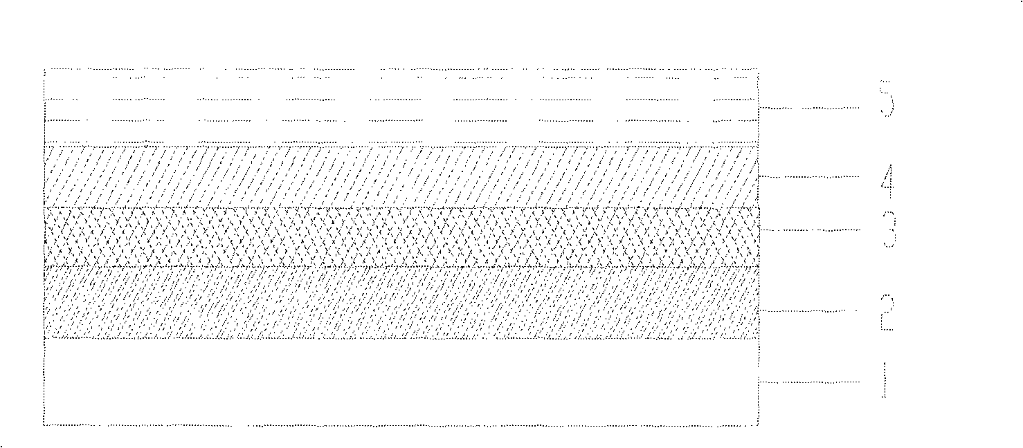
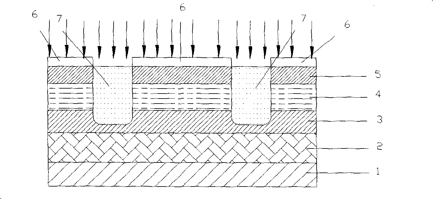
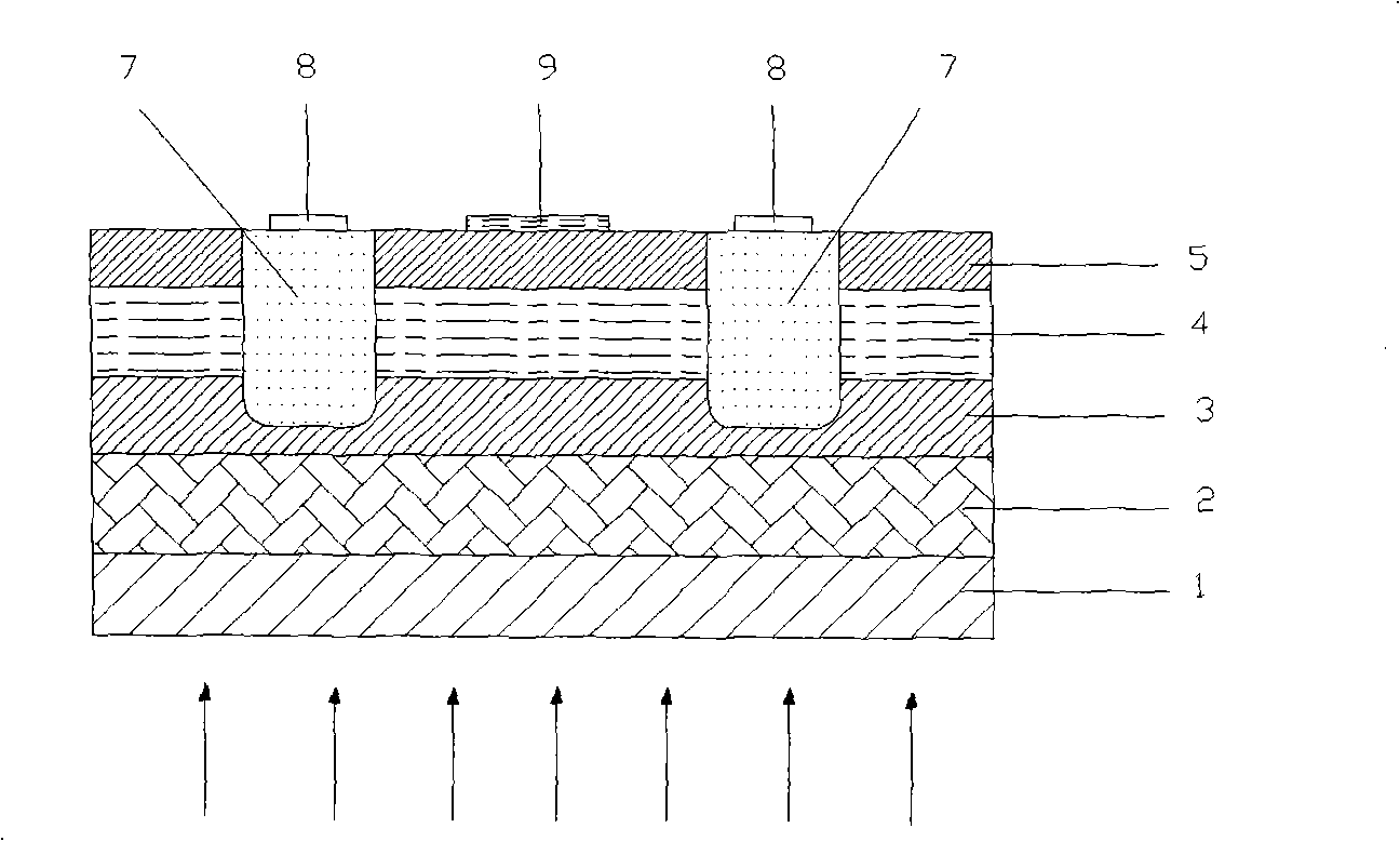
[0030] The structure of the back-illuminated planar PIN structure GaN-based ultraviolet detector as shown in the accompanying drawing of the figure description is to epitaxially grow a layer of about 0.6 micron thick undoped Doped AlN buffer layer 2; about 1 micron thick Si doping concentration is 1×10 18 cm -3 n-type Al 0.3 Ga 0.7 N layer 3; active layer 4 is an intrinsic GaN layer with a thickness of about 0.15 microns and an electron concentration of 2×10 16 cm -3 ; Finally, a Mg-doped p-GaN layer 5 with a thickness of about 0.1 micron, with a hole concentration of about 2×10 17 cm -3 . Use a high-energy ion implanter to i...


PUM

PropertyMeasurementUnit
Thicknessaaaaaaaaaa
Electron concentrationaaaaaaaaaa
Thicknessaaaaaaaaaa

Abstract

The invention discloses a GaN based ultraviolet detector of a back illumination plane type PIN structure, which is characterized by comprising a substrate, an AlN buffer layer, an Si doped n type AlxGa1-xN (x is more than 0 and less than or equal to 0.8) layer, an active layer that is an intrinsic and weak n doped GaN layer, and a p type ohmic contact layer that is an Mg doped p type GaN. An n type groove is prepared by Si ion injection process and is communicated with the n type AlxGa1-xN (x is more than 0 and less than or equal to 0.8) layer, the active layer and the p type ohm contact layer. The detector further comprises an n type ohmic contact electrode that is manufactured on the n groove and a p type ohm contact electrode that is manufactured on the p type ohm contact layer, so as to constitute the GaN based ultraviolet detector of the back illumination plane type PIN structure.

Description

technical field [0001] The invention relates to ultraviolet detector technology, in particular to a back-illuminated planar PIN structure GaN-based ultraviolet detector and a preparation method. Background technique [0002] GaN-based wide-bandgap semiconductor materials have great potential and reality in high-power, high-frequency electronic devices, light-emitting devices, and ultraviolet detectors due to their stable chemical properties, direct bandgap, and large adjustable bandgap range. application. And since several key processes have made great breakthroughs: first, before growing GaN, a two-step growth method of growing a layer of AlN or GaN buffer layer on the substrate at low temperature has obtained high-quality GaN single crystal thin film; It is the acquisition of p-type GaN and the clarification of the reasons why p-type has not been realized before, which makes the research of GaN-based ultraviolet detectors a hot spot. [0003] So far, many GaN-based ultra...

Claims


Application Information

Patent Timeline
IPC IPC(8): H01L31/04H01L31/18H01L31/0224H01L31/105
CPCY02E10/50
Inventor 包西昌张文静许金通王玲李超储开慧王妮丽张燕李向阳
Owner SHANGHAI INST OF TECHNICAL PHYSICS - CHINESE ACAD OF SCI
Features
  • Generate Ideas
  • Intellectual Property
  • Life Sciences
  • Materials
  • Tech Scout
  • Unparalleled Data Quality
  • Higher Quality Content
  • 60% Fewer Hallucinations
Learn More