
Gallium nitride LED

A light-emitting diode, gallium nitride-based technology, applied in the direction of electrical components, circuits, semiconductor devices, etc., can solve the problems of poor adhesion of epitaxial layers, etc., and achieve the effect of solving poor adhesion and improving reliability

Inactive Publication Date: 2009-07-29
XIAMEN SANAN OPTOELECTRONICS TECH CO LTD
View PDF1 Cites 5 Cited by
  • Summary
  • Abstract
  • Description
  • Claims
  • Application Information

AI Technical Summary

Problems solved by technology

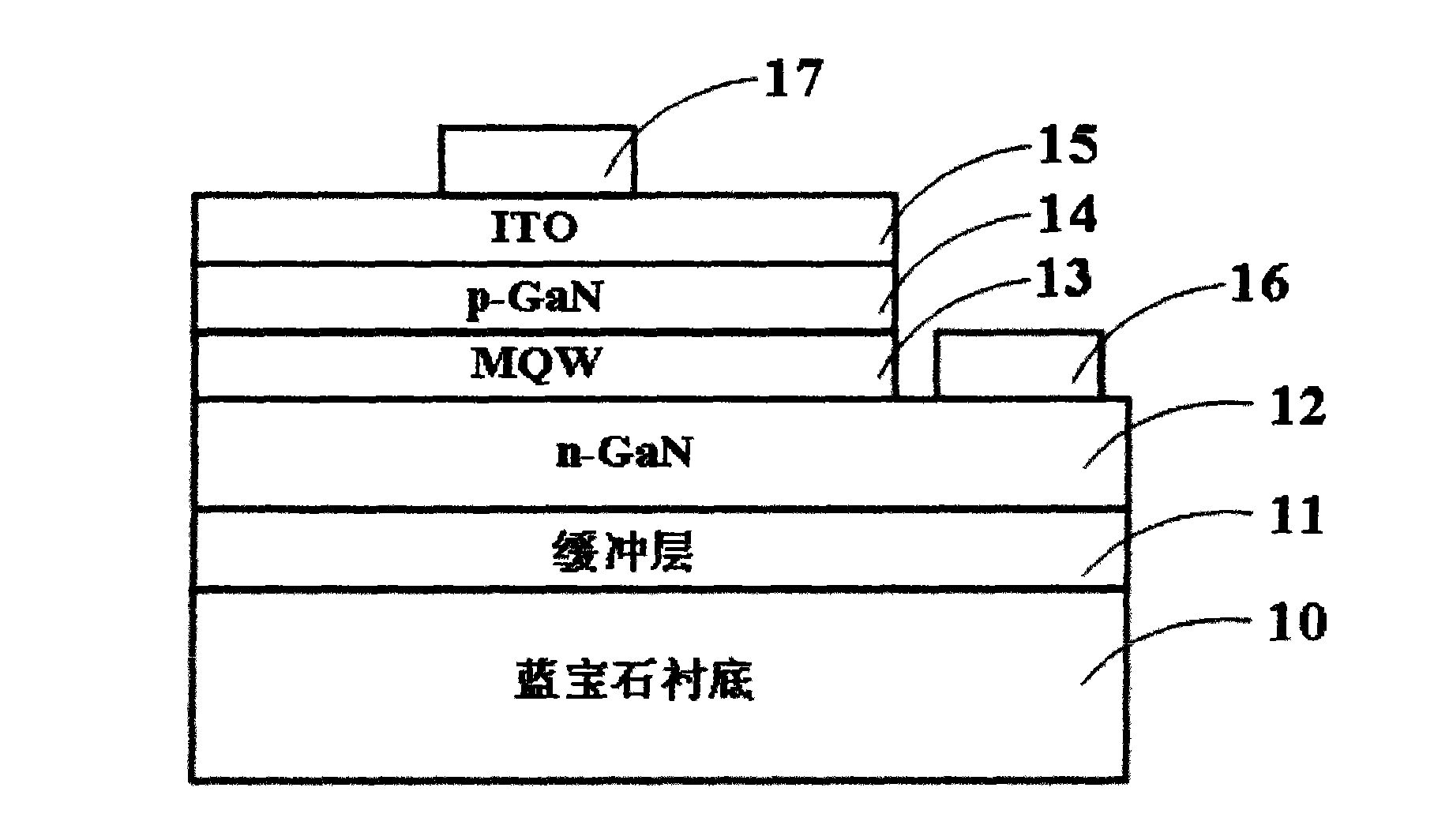
[0004] In order to solve the problem of poor adhesion between ITO and the p-type GaN-based epitaxial layer and improve the reliability of gallium nitride-based light-emitting diodes, the present invention aims to provide a gallium nitride-based light-emitting diode

Method used


Image

  • Gallium nitride LED
  • Gallium nitride LED

Examples


Embodiment Construction

[0024] The present invention will be further described below in conjunction with the drawings and embodiments.

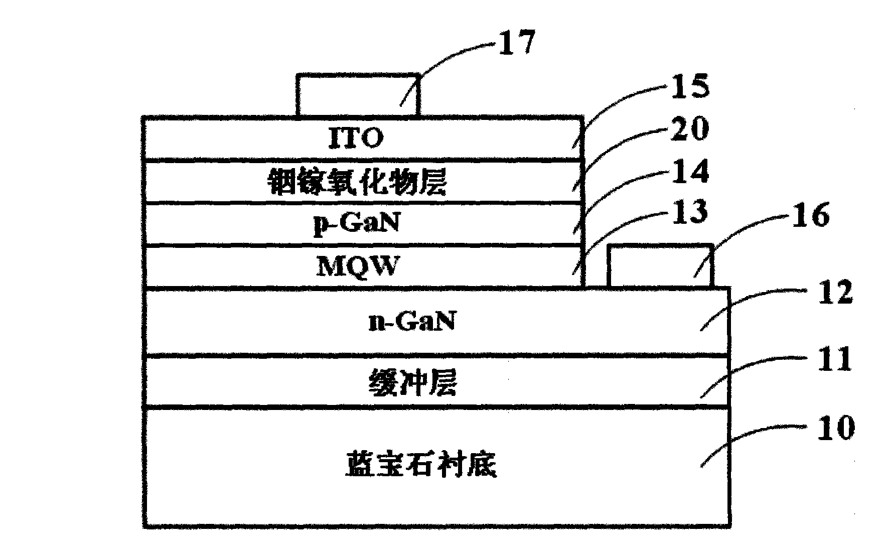
[0025] As attached figure 2 A gallium nitride-based light-emitting diode structure shown, sapphire substrate 10, buffer layer 11, n-GaN layer 12, multiple quantum well active layer 13, p-GaN layer 14, indium gallium oxide layer 20, ITO Layer 15, p-electrode 17, and n-electrode 16.

[0026] Among them, the bottom layer is a sapphire substrate 10; the buffer layer 11 is formed on the sapphire substrate 10, and its material can be aluminum gallium indium Al 1-x-y Ga x In y N (0≤x<1, 0≤y<1); the n-GaN layer 12 is formed on the buffer layer 11; the multiple quantum well active layer 13 is formed on the n-GaN layer 12, the material of which is nitrided Indium gallium (InGaN); the p-GaN layer 14 is formed on the multiple quantum well active layer 13; the indium gallium oxide layer 20, that is, the mixture layer of indium oxide and gallium oxide is formed on the p-GaN layer 14,...


PUM


Abstract

The invention discloses a gallium-nitride-based (GaN-based) luminescent diode. The luminescent diode comprises a sapphire substrate, a buffering layer, an n-type GaN-based extension layer, an active layer, a p-typed GaN-based extension layer, an adhesive layer, an ITO layer, a p electrode and an n electrode, wherein, the bottommost layer is the sapphire substrate; the buffering layer is formed on the sapphire substrate, the n-type GaN-based extension layer is formed on the buffering layer; the active layer is formed on the GaN-based extension layer and the material of the active layer is GaN; the p-type GaN-based extension layer is formed on the active layer; a layer of oxides of indium and gallium is the adhesive layer formed on the p-type GaN-based extension layer; the p electrode is formed on the ITO layer, and the n electrode is formed on the GaN-based extension layer. The introduction of the layer of oxides of indium and gallium between the ITO and the p-type GaN-based extension layer solves the poor adhesiveness between the ITO and the p-type GaN-based extension layer and improves the reliability of the gallium nitride-based (GaN-based) luminescent diode.

Description

Technical field [0001] The invention relates to a light-emitting diode, in particular to a gallium nitride-based light-emitting diode. Background technique [0002] At present, gallium nitride (GaN)-based light-emitting diodes (LEDs) have been widely used in the fields of mobile phone buttons, indications, displays, backlights, and lighting; as various applications increase the brightness requirements of GaN-based LED devices, the existing technology usually A transparent conductive oxide (TCO) is used to replace the early semi-transparent Ni / Au as the transparent contact layer of the p-type GaN-based epitaxial layer to improve the luminous efficiency. Indium tin oxide (ITO) is by far the most widely used TCO in GaN-based LEDs, among which the US patent US6078064 is a typical representative of the existing technology. [0003] Such as figure 1 A GaN-based light-emitting diode structure using the prior art includes: a sapphire substrate 10, a buffer layer 11, an n-GaN layer 12, a...

Claims


Application Information

Patent Timeline
IPC IPC(8): H01L33/00
Inventor 潘群峰吴志强林科闯
Owner XIAMEN SANAN OPTOELECTRONICS TECH CO LTD
Learn More