Metal mold for injection molding and semiconductor package formed therewith and method of manufacturing semiconductor package
An injection molding, semiconductor technology, applied in the direction of semiconductor/solid-state device manufacturing, semiconductor devices, semiconductor/solid-state device components, etc., can solve the problems of easy to produce weld lines, unfilled molding, short shots, etc.
- Summary
- Abstract
- Description
- Claims
- Application Information
AI Technical Summary
Problems solved by technology
Method used
Image

Examples
Embodiment approach 1
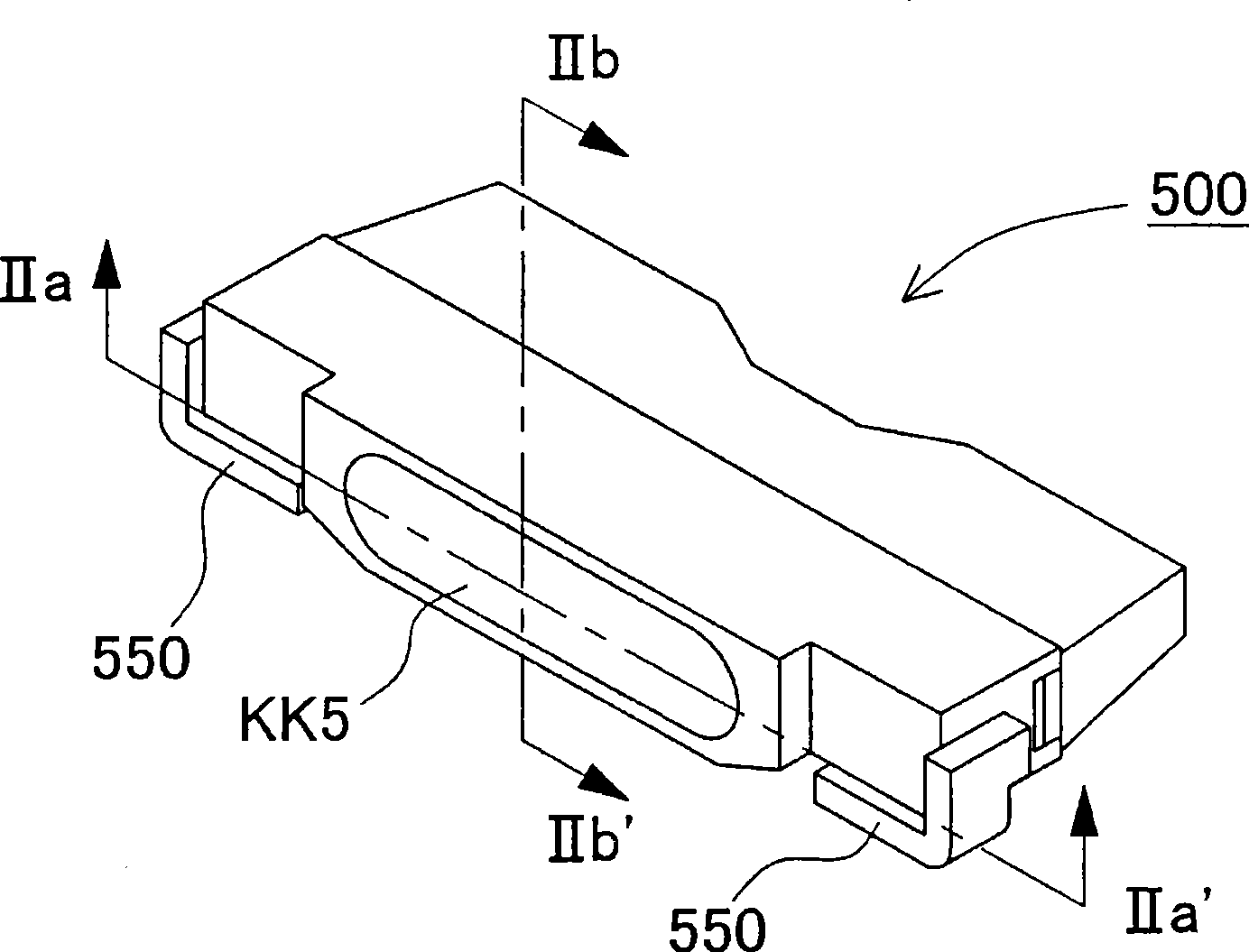
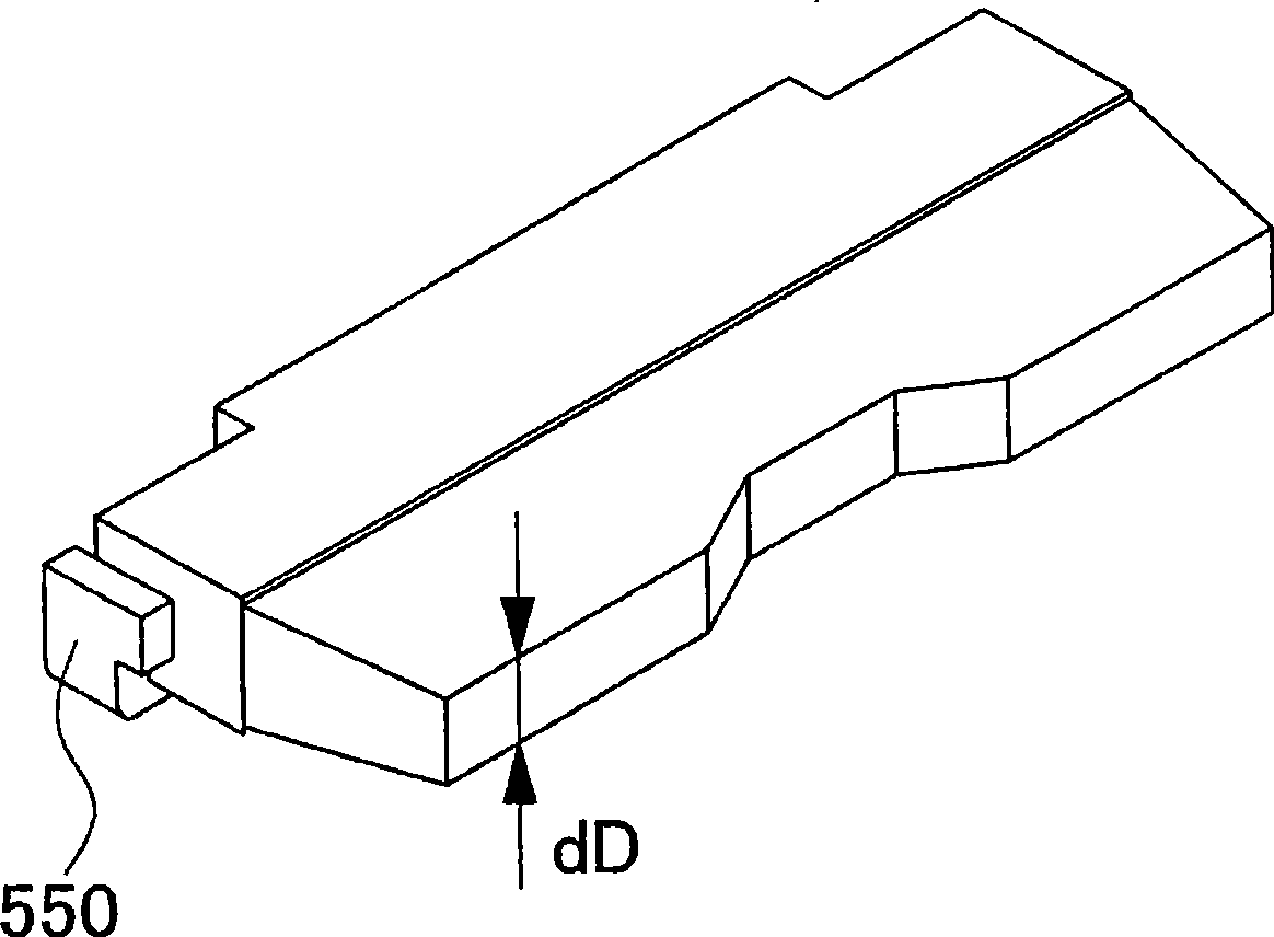
[0050] exist image 3 ˜ FIG. 7 show the appearance of the semiconductor package 100 according to Embodiment 1 of the present invention. In these figures, image 3 is a perspective view showing the semiconductor package 100 viewed obliquely from above, Figure 4 It is a perspective view showing obliquely downward viewing from the front, Figure 5 It is a perspective view showing obliquely upward observation from the rear, Figure 6 It is a perspective view showing obliquely downward observation from the rear, Figure 7A represents the main view, Figure 7B represents the rear view, Figure 7C It is a side view showing a section of the box-shaped block 11 (front-side sealing). The semiconductor package 100 shown in these figures is a side-emission type light-emitting device using a semiconductor light-emitting element 30, and includes: a resin-molded package body 10 thinner than its width; external electrodes 50 .
[0051] (lead frame 20)
[0052] A lead frame 20 is bur...
Embodiment approach 2
[0083] In addition, the shape of the semiconductor package is not limited to the above configuration, and various configurations can be used. As an example, in Figure 12 to Figure 15 An example of the semiconductor package 200 in which the shape of the external electrodes of the second embodiment is changed is shown in . In these figures, Figure 12 is a perspective view showing the semiconductor package 200 viewed obliquely from above, Figure 13 It is a perspective view showing obliquely downward viewing from the front, Figure 14It is a perspective view showing obliquely upward observation from the rear, Figure 15 It is a perspective view showing obliquely downward viewing from the rear. The semiconductor package 200 shown in these figures is also the same as the first embodiment, and is a side-emission light-emitting device using a semiconductor light-emitting element, and the same reference numerals are assigned to common components, and detailed description thereof...
Embodiment 1
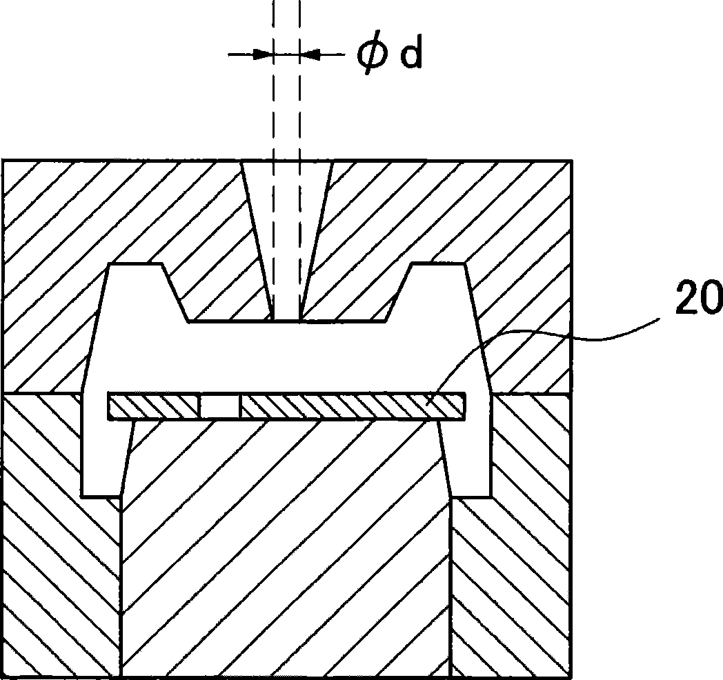
[0103] As Example 1, produced such as Figure 16 The shown injection molding mold 60 is composed of a fixed mold 61 , a movable mold 62 , and a mold insert 63 . The gate 65 formed on the fixed mold 61 gradually becomes thinner from the side of the runner 64 to the side of the cavity 68 to the top of the cavity 68 , and passes through from the top of the cavity 68 within the range that does not exceed the outermost contour of the movable mold 62 . , extending to the side of the fixed mold 61, obtaining a size to become the outermost contour in one direction, and extending to the joint surface 108 of the fixed mold 61 at the same time. By adopting such a shape of the gate 65 , it is possible to have a gate with the largest diameter when manufacturing a semiconductor package of the same shape with the injection mold 60 . The larger the gate diameter Φd1, the longer the time for the molten resin JS to cool and solidify. Therefore, the injection molding die 60 can be the most diff...
PUM
| Property | Measurement | Unit |
|---|---|---|
| Thermal conductivity | aaaaa | aaaaa |
| Diameter | aaaaa | aaaaa |
| Thickness | aaaaa | aaaaa |
Abstract
Description
Claims
Application Information
 - R&D
- Intellectual Property
- Life Sciences
- Materials
- Tech Scout
- Unparalleled Data Quality
- Higher Quality Content
- 60% Fewer Hallucinations
Browse by: Latest US Patents, China's latest patents, Technical Efficacy Thesaurus, Application Domain, Technology Topic, Popular Technical Reports.
© 2025 PatSnap. All rights reserved.Legal|Privacy policy|Modern Slavery Act Transparency Statement|Sitemap|About US| Contact US: help@patsnap.com