Mixer circuit, semiconductor apparatus including the same, communication device including the same, and electronic device including the same

A technology of frequency mixing circuit and communication device, which is applied to the modulation conversion of semiconductor devices with at least two electrodes, the balance device of modulation conversion, electrical components, etc., can solve the problems of single-band broadcast audio-visual obstacles, deterioration of reception performance, etc.

Inactive Publication Date: 2009-08-12
SHARP KK
View PDF1 Cites 3 Cited by
  • Summary
  • Abstract
  • Description
  • Claims
  • Application Information

AI Technical Summary

Problems solved by technology

In the case where the above-mentioned unwanted signal overlaps at a high level with the same frequency as the TV broadcast signal, the reception performance deteriorates significantly compared to the case where the above-mentioned unwanted signal appears at a different frequency
[0036] In addition, when receiving 650MHz digital TV broadcasting, since the 1950MHz W CDMA interference wave satisfies f U = 3f D , therefore, resulting in audio-visual impairment of single-segment broadcasting

Method used


Image

  • Mixer circuit, semiconductor apparatus including the same, communication device including the same, and electronic device including the same
  • Mixer circuit, semiconductor apparatus including the same, communication device including the same, and electronic device including the same
  • Mixer circuit, semiconductor apparatus including the same, communication device including the same, and electronic device including the same

Examples


Embodiment Construction

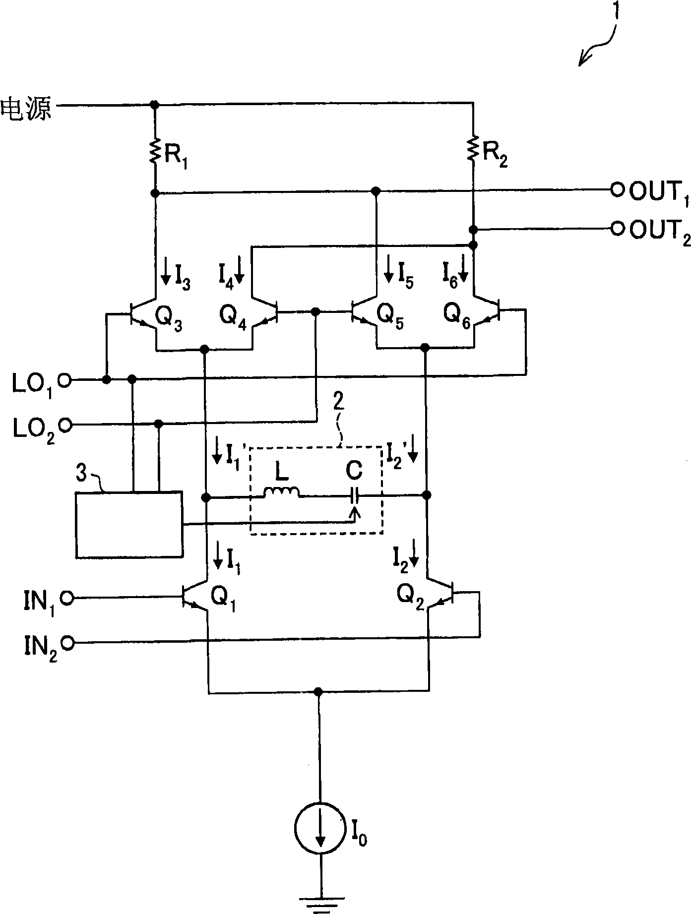
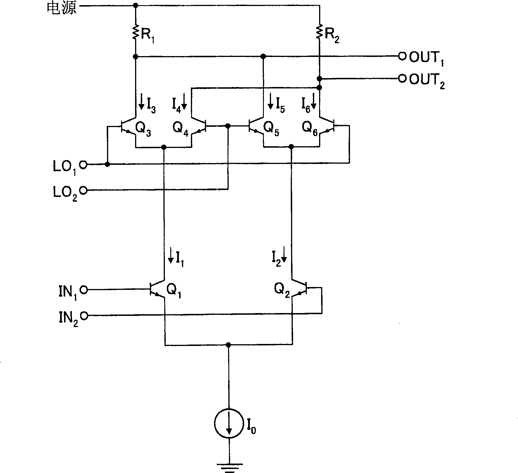
[0043] Below, according to figure 1 One embodiment of the present invention will be described.

[0044] figure 1 It is a circuit diagram showing the mixer circuit 1 according to the embodiment of the present invention. Mixing circuit 1 includes: transistor Q 1 Q 6 ; Load resistance R 1 , R 2 ; current source I 0 ; Inductor L and capacitor C.

[0045] input signal IN 1 Input Transistor Q 1 base of the inverting input signal IN 2 Input Transistor Q 2 base.

[0046] Local oscillator signal LO 1 Input Transistor Q 3 base of transistor Q 6 base, inverting the local oscillator signal LO 2 Input Transistor Q 4 base of transistor Q 5 base.

[0047] Transistor Q 1 emitter, transistor Q 2 emitter with a common current source I 0 connected to the input of the current source I 0 The output terminal is electrically grounded.

[0048] Transistor Q 1 The collector of the transistor Q 3 emitter as well as the transistor Q 4 The emitter connection of the transistor ...


PUM


Abstract

A mixer circuit 1 is a mixer circuit including a pair of differential transistors which receives an input signal IN1-IN2; and a serial resonance circuit 2 connected between collectors of transistors Q1 and Q2 of the pair of differential transistors, the mixer circuit mixing the input signal IN1-IN2 and a local signal LO1-LO2, and outputting the mixed signal.

Description

technical field [0001] The present invention relates to a frequency mixing circuit, a semiconductor device, a communication device, and electronic equipment including the frequency mixing circuit. Background technique [0002] figure 2 Indicates an existing mixer circuit. [0003] input signal IN 1 Input Transistor Q 1 The base of the inverting input signal (inverting input signal) IN 2 Input Transistor Q 2 base. [0004] Local oscillator signal LO 1 Input Transistor Q 3 base of the transistor Q 6 base, inverting the local oscillator signal LO 2 Input Transistor Q 4 base of the transistor Q 5 base. [0005] Transistor Q 1 emitter, transistor Q 2 emitter with a common current source I 0 connected to the input of the current source I 0 The output terminal is electrically grounded. [0006] Transistor Q 1 The collector of the transistor Q 3 emitter as well as the transistor Q 4 The emitter connection of the transistor Q 2 The collector of the transistor Q ...

Claims


Application Information

Patent Timeline
Patent Type & Authority Applications(China)
IPC IPC(8): H03D7/12H03D7/00H03D7/14
CPCH03D7/1458H03D2200/0025H03D7/1425H03D7/1433
Inventor 久保田晋平
Owner SHARP KK
Why Eureka
Try Eureka