Interface circuit and method for suppressing electromagnetic interference

An electromagnetic interference and interface circuit technology, applied in the direction of reducing electrical interference, line transmission components, and improving frequency characteristics, can solve the problems of reduced isolation performance of transformers, strong electromagnetic interference, etc. The effect of loop performance

Inactive Publication Date: 2009-08-12
HUAWEI DEVICE (SHENZHEN) CO LTD
View PDF0 Cites 7 Cited by
  • Summary
  • Abstract
  • Description
  • Claims
  • Application Information

AI Technical Summary

Problems solved by technology

Due to the small impedance of capacitors C1 and C3 to high-frequency signals, high-frequency signals are coupled to the copper wire loop through capacitors C1 and C3, and external surges (such as lightning strikes) are easily coupled to the copper wire loop through capacitors C1 and C3. In the equipment of the circuit, the isolation performance of the transformer is reduced, resulting in strong electromagnetic interference

Method used


Image

  • Interface circuit and method for suppressing electromagnetic interference
  • Interface circuit and method for suppressing electromagnetic interference
  • Interface circuit and method for suppressing electromagnetic interference

Examples


Embodiment 1

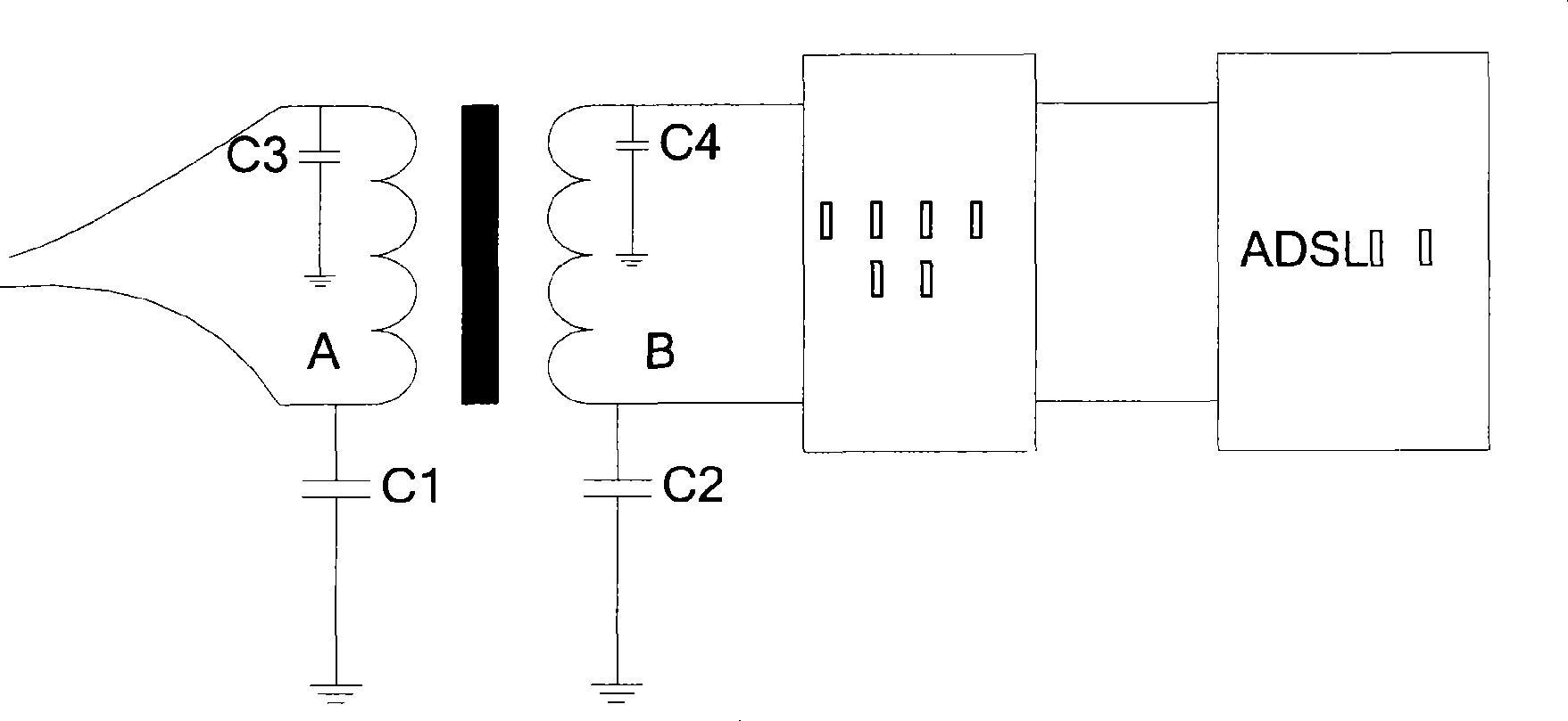
[0034] Such as Figure 5 As shown, in this embodiment, two secondary coils are set on the transformer of the interface circuit, one primary coil, one secondary coil is the sending port, the other secondary coil is the receiving port, and the two secondary coils There is a DC blocking capacitor in series in the middle, so both ends of the DC blocking capacitor need to be grounded through the filter capacitor, such as Figure 5 C1, C2, C3 and C4 in . In this embodiment, a signal terminal 1 of the transmitting port is grounded through the distributed capacitance between 1 and 3 on the secondary coil and the filter capacitor C3, so that the high-frequency noise reaching the signal terminal 1 is guided to the ground terminal.

[0035] Similarly, the other signal terminal 4 of the transmitting port, and the high-frequency noise at the two signal terminals (5 and 8 ) of the receiving port are also guided to the ground terminal. This embodiment prevents high-frequency noise from bei...

Embodiment 2

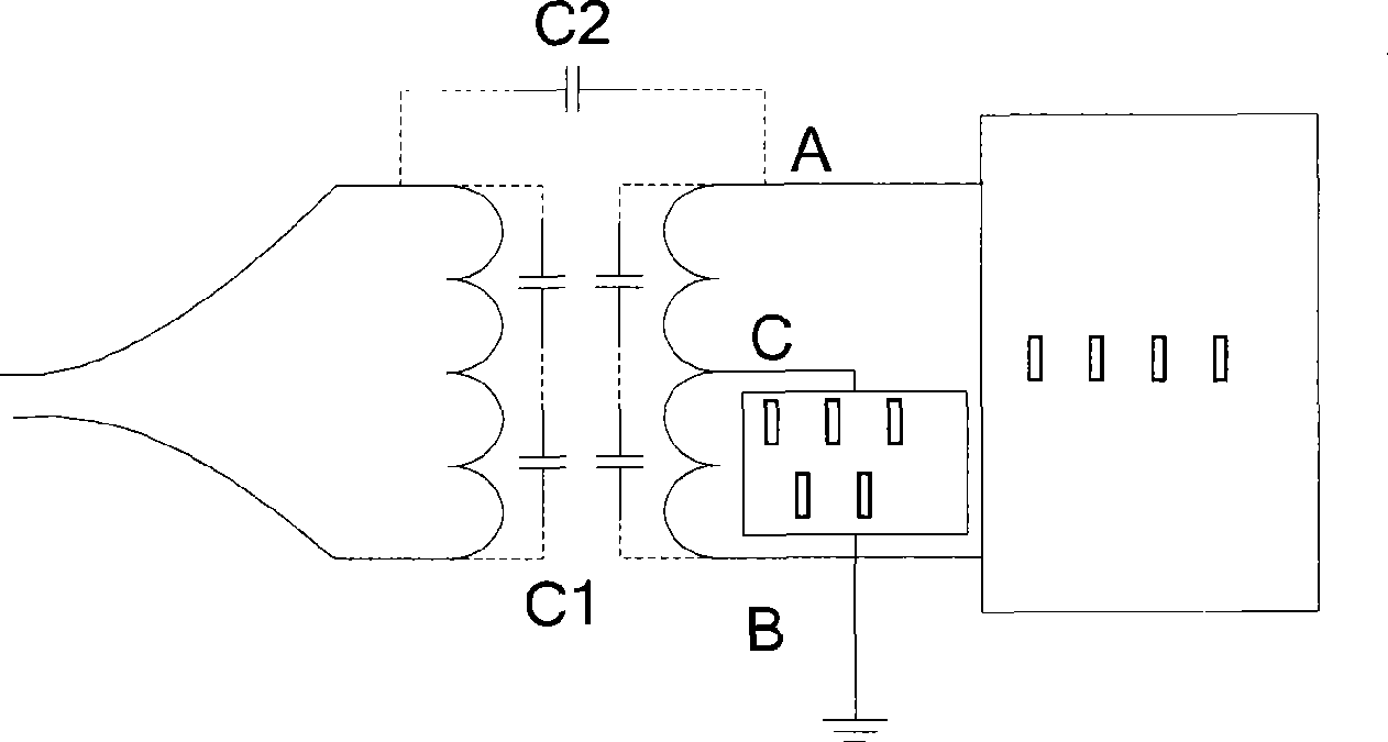
[0040] Such as Figure 7 As shown, the transformer of the interface circuit in this embodiment is provided with two secondary coils, one primary coil, one secondary coil is the sending port, and the other secondary coil is the receiving port, but only in the middle of the secondary coil of the sending port DC blocking capacitors are connected in series. For the transmitting port, both ends of the DC blocking capacitor need to be grounded through filter capacitors (C5 and C6), while the receiving port only needs to be grounded through a filter capacitor C7 in the middle of the coil.

[0041] Same as the principle in Embodiment 1, this embodiment prevents high-frequency noise from being input to the chip connected to the interface circuit, thereby ensuring that the signal input to the chip will not affect the working performance of the chip.

[0042] It can be concluded that after adopting the embodiment of the present invention, the high-frequency noise of the interface circui...

Embodiment 3

[0046] The high-frequency filter used in this embodiment is different from the high-frequency filter used in Embodiment 1 and Embodiment 2. In Embodiment 1 and Embodiment 2, analog filters are used, and digital filters can be used instead of analog filters in practical applications.

[0047] In general, digital filters are completed by DSP (Digital Signal Processing) chips and corresponding programs. The specific process is as follows: first perform FFT transform (Fast Fourier Transform) on the signal, and then multiply the transformed signal by a frequency Factor, in order to filter out unwanted frequency signals, and finally perform DFT transform (inverse fast Fourier transform) to obtain the output signal.


PUM


Abstract

The embodiment of the invention discloses an interface circuit and a method for inhibiting electromagnetic interference, which relate to interface circuits of communication equipment, and are mainly used for equipment such as ADSL and ISDN performing communication through copper wire loops. The interface circuit for inhibiting electromagnetic interference comprises a transformer, the transformer comprises a primary coil and a secondary coil, the secondary coil is provided with an intermediate tap, and the intermediate tap is earthed through a high frequency filter. The method for inhibiting electromagnetic interference conducts high frequency noise to an earthing point through the high frequency filter on the intermediate tap of the secondary coil of the transformer, thereby filtering the high frequency noise. The interface circuit and the method solve the problem that an interface circuit of the prior communication equipment has weaker electromagnetic interference inhibition function.

Description

technical field [0001] The invention relates to an interface circuit of a communication device, in particular to an interface circuit with the function of suppressing electromagnetic interference in the communication device, and a method for suppressing electromagnetic interference by the interface circuit. Background technique [0002] Using general digital transmission technology on existing copper wire loops can make the digital transmission rate of most copper wire loops reach 9.6kbits or even 28.8kbit / s; if DSL (Digital Subscriber Loop) technology is used, it can make The digital transmission rate of the copper wire loop can reach MHz level. [0003] In order to achieve full-duplex operation (that is, the transmit channel and the receive channel work at the same time) in the copper wire loop, the modem divides the passband into two separate channels for upstream and downstream communications, and uses a callback cancellation circuit, Finally, through a transformer, the...

Claims


Application Information

Patent Timeline
IPC IPC(8): H04B3/26H04B15/02
Inventor 狄伟
Owner HUAWEI DEVICE (SHENZHEN) CO LTD
Why Eureka
Try Eureka