Data-latching circuit adopting phase selector

A technology of phase selector and data latch, applied in multiple input and output pulse circuits, delay line pulse generation, etc., can solve the problems of sampling error, lock circuit 100 data error, and failure to guarantee correctness, etc.

Active Publication Date: 2009-09-02
REALTEK SEMICON CORP
View PDF0 Cites 7 Cited by
  • Summary
  • Abstract
  • Description
  • Claims
  • Application Information

AI Technical Summary

Problems solved by technology

However, if the setup time and data hold time of the flip-flop are not enough, the lock circuit 100 still has the problem of data error, such as figure 2 shown, when flip-flop 104 samples data D 1 to get data D 2 , if the flip-flop 102 is sampling the input data D in , then due to the data D 1 The logic value of is changing, so the data D obtained by flip-flop 104 2 It cannot be guaranteed to be correct

Method used


Image

  • Data-latching circuit adopting phase selector
  • Data-latching circuit adopting phase selector
  • Data-latching circuit adopting phase selector

Examples


Embodiment Construction

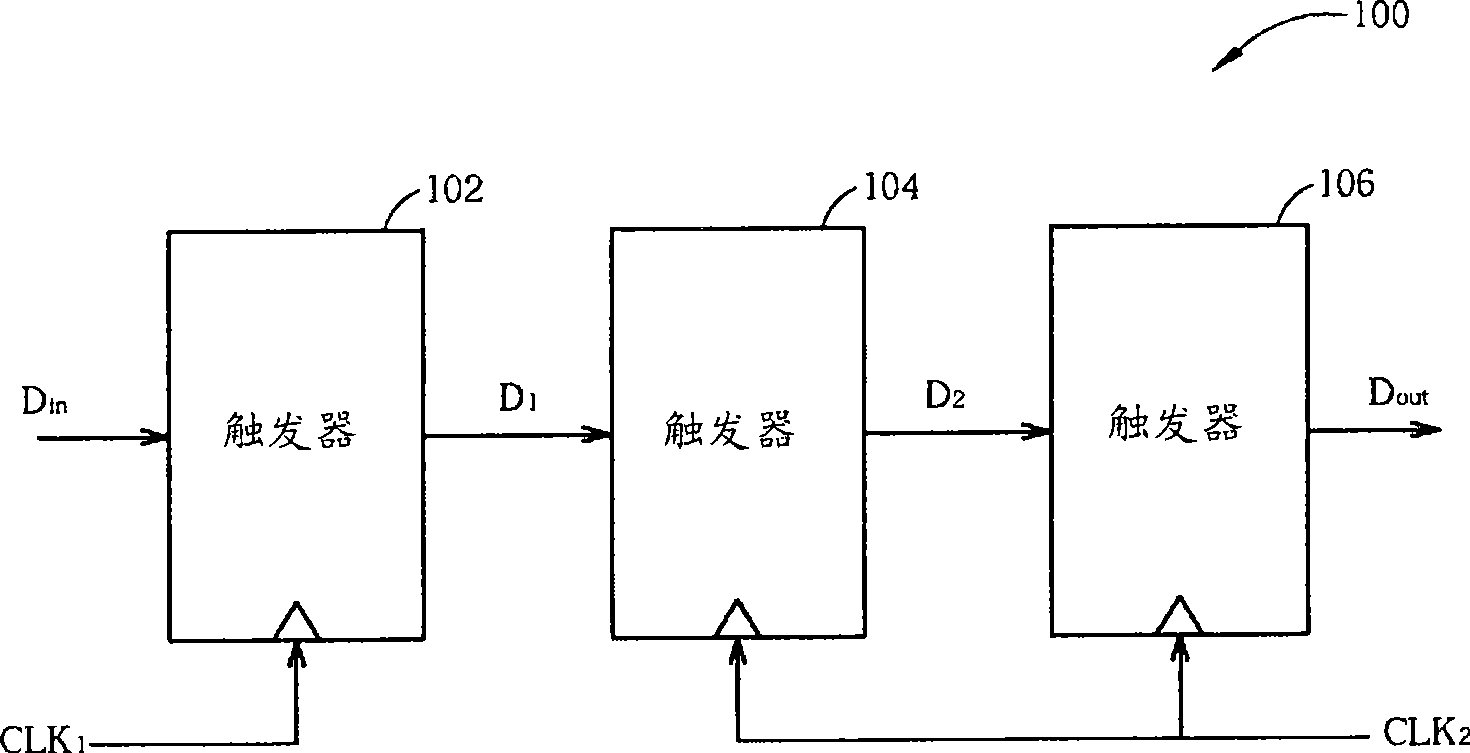
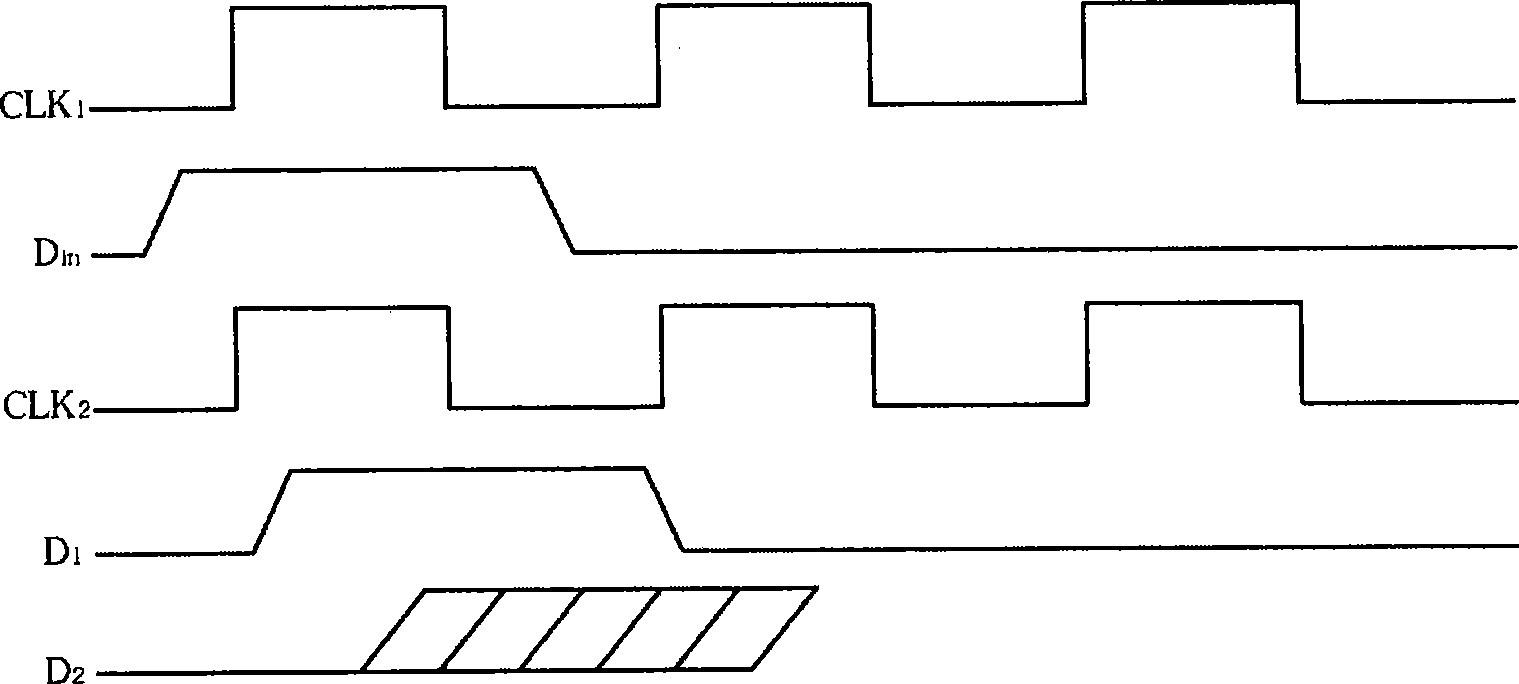
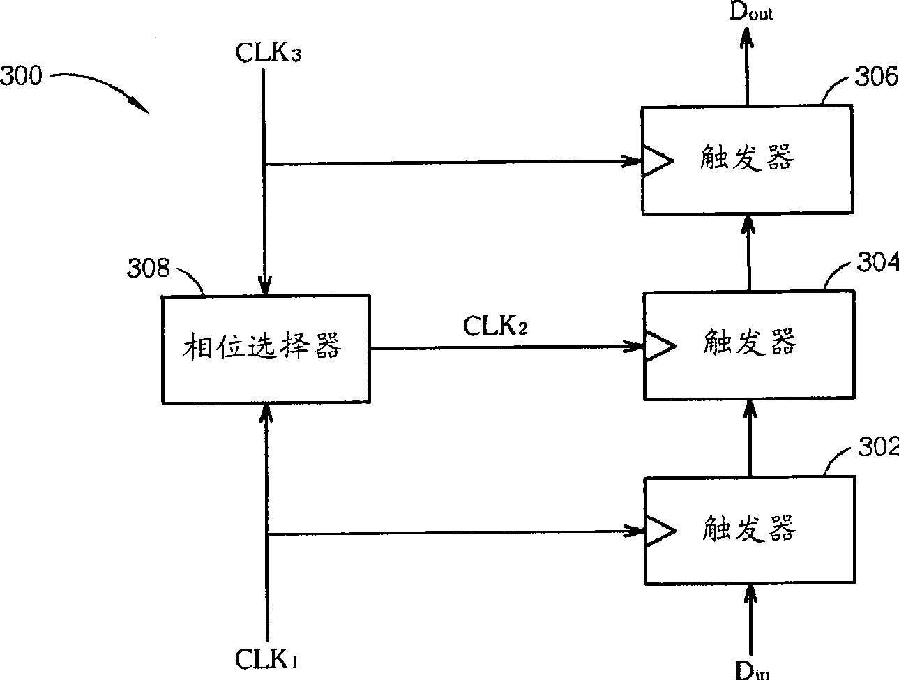
[0017] see image 3 , image 3 It is a schematic diagram of an embodiment of the data latch circuit 300 of the present invention. In this embodiment, the data latch circuit 300 includes three series-connected flip-flops (such as D-type flip-flops) 302, 304, 306 and a phase selector 308, wherein the input data D in The flip-flop 302 is clocked by a first CLK 1 to trigger, and the flip-flop 306 that finally generates output data is controlled by another third clock CLK 3 to trigger. For the flip-flop 304 in the middle, it is driven by a second clock CLK 2 triggered, and the second clock CLK 2 is determined by the phase selector 308 according to the first clock CLK 1 with the third clock CLK 3 The phase relationship between them is generated. In this embodiment, the phase selector 308 is based on the first clock CLK 1 with the third clock CLK 3 phase relationship between to selectively use the third clock CLK 3 or third clock CLK 3 The inverted signal is used as the se...


PUM


Abstract

The invention provides a data-latching circuit. The data-latching circuit comprises a first data-latching unit, a second data-latching unit, a third data-latching unit and a phase selector, wherein the first data-latching unit is used for latching a first input data according to a first clock signal and outputting a first output data; the second data-latching unit is used for latching the first output data according to a second clock signal and outputting a second output data; the third data-latching unit is used for latching the second output data according to a third clock signal and outputting an output data; and the phase selector is coupled with the second data-latching unit and used for generating the second clock signal according to the phase relation between the first and the third clock signals and outputting the second clock signal to the second data-latching unit.

Description

technical field [0001] The invention relates to a data receiving device and method, in particular to a data latch circuit and method using a phase selector. Background technique [0002] In some interface systems or larger chips, maintaining the same clock in each part of the chip is the biggest challenge to the system. Usually, the existing chips contain digital circuit parts and analog circuit parts, and the digital circuit part occupies almost 100% of the chip. Mainly more than 80% of the area, so when the circuit designer plans the timing problem of the entire integrated circuit, it is usually the digital circuit design to estimate the driving capability of the clock output from the digital circuit part and the capacitance generated by the circuit layout and routing effect, and by analyzing and estimating the delay between the clock that finally reaches the analog circuit part and the clock output by the original clock source, and finally solves the problem of clock phas...

Claims


Application Information

Patent Timeline
IPC IPC(8): H03K3/86H03K5/26
Inventor 徐建昌
Owner REALTEK SEMICON CORP
Why Eureka
Try Eureka