Process for producing nitride semiconductor, crystal growth rate enhancement agent, nitride single crystal, wafer and device

A technology of nitride semiconductors and manufacturing methods, which is applied in semiconductor/solid-state device manufacturing, single crystal growth, single crystal growth, etc., and can solve problems such as different growth rates, impurity concentrations, and number of crystal defects, and the inability to obtain uniform quality wafers, etc. , to achieve the effect of increased growth rate, excellent quality and homogeneous quality

Inactive Publication Date: 2009-09-02
MITSUBISHI CHEM CORP +1
View PDF10 Cites 15 Cited by
  • Summary
  • Abstract
  • Description
  • Claims
  • Application Information

AI Technical Summary

Problems solved by technology

[0017] In addition, in order to obtain a wafer with a large M plane, a method is employed in which an M plane wafer is cut from a bulk gallium nitride single crystal obtained by crystal growth along the c-axis direction by an ammonothermal method or the like. However, in this method, On the C+ face and the C- face, the growth rate is different, so there is a problem that the impurity concentration and the number of crystal defects in the C+ face growth part and the C- face growth part on the both end faces of the obtained crystal are different, and the Wafers with uniform quality in the M plane

Method used


Image

  • Process for producing nitride semiconductor, crystal growth rate enhancement agent, nitride single crystal, wafer and device
  • Process for producing nitride semiconductor, crystal growth rate enhancement agent, nitride single crystal, wafer and device
  • Process for producing nitride semiconductor, crystal growth rate enhancement agent, nitride single crystal, wafer and device

Examples


Embodiment 1

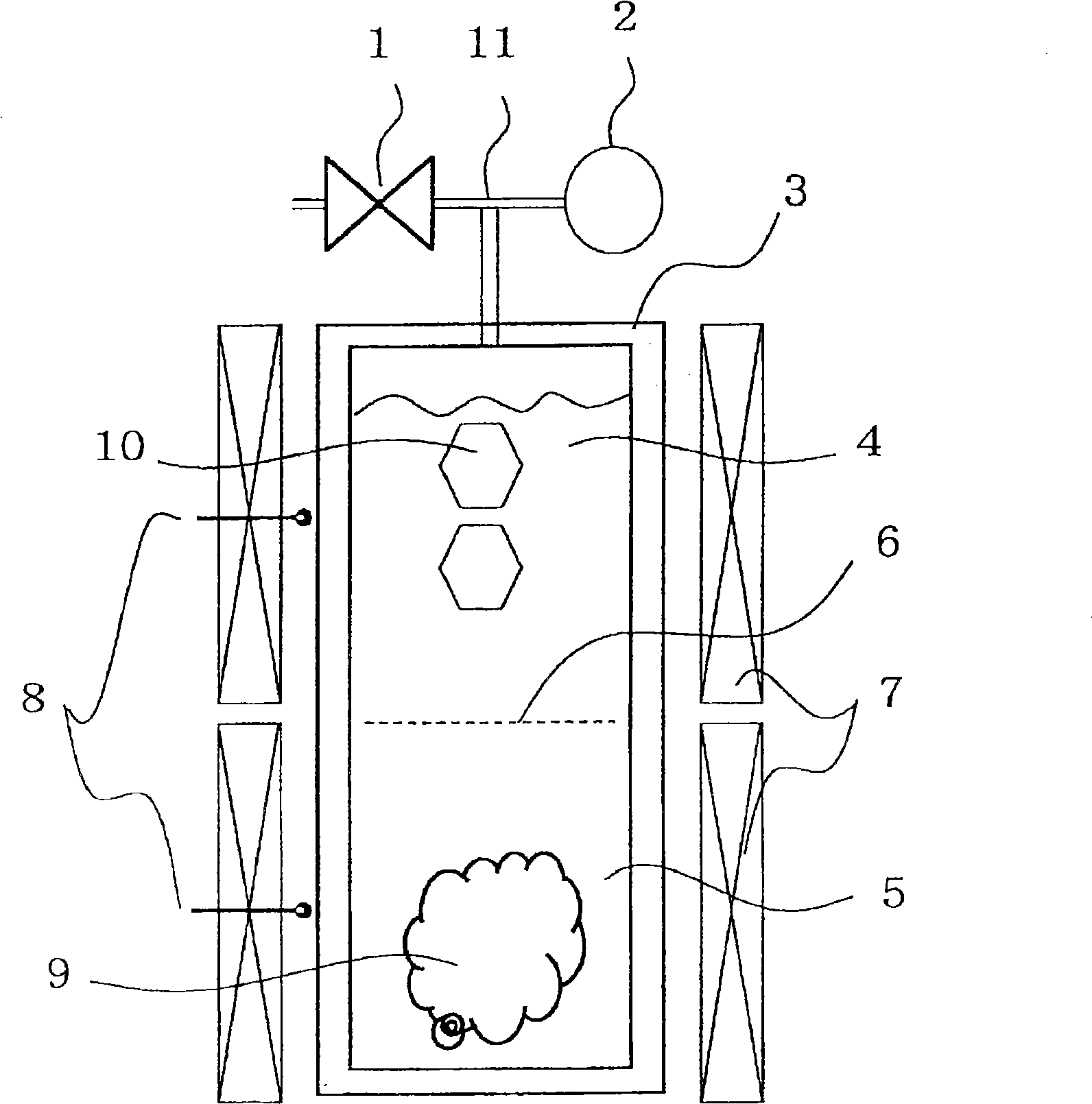
[0126] use figure 2 The shown setup was used for crystal growth.

[0127] Using a platinum-lined autoclave 3 (manufactured by Incone 1625, about 30 ml) with an internal size of 16 mm in diameter and 160 mm in length, 7.4 g of GaN polycrystals produced by HVPE were charged as a raw material 9 into the raw material filling part 5 of the autoclave, and then Filled with fully dried powdered NH 4 Cl (purity 99.99%) 1.57g was used as a mineralizer.

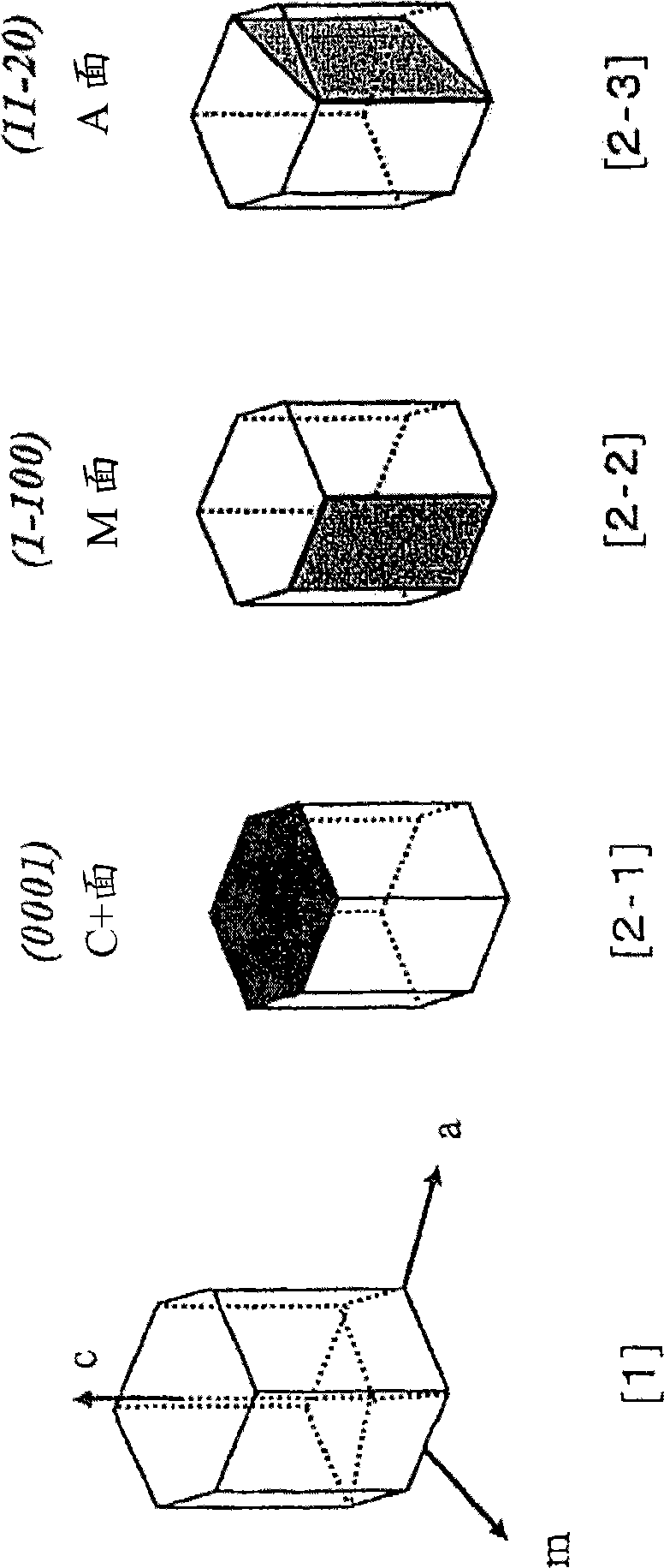
[0128] Next, the baffle 6 was placed at a position 80 mm from the bottom, and GaN seed crystals were placed on the crystal growth portion 4 thereon, and the lid of the autoclave equipped with a valve was quickly closed, and then the measurement of the autoclave 3 was performed. The GaN seed crystal 10 used here has a thickness of 50 μm in the c-axis direction, a C-plane of 5 mm square, and one of the sides becomes an M-plane by cleavage. Next, the operation is to connect the conduit 11 to the vacuum pump through the valve 1 attached...

Embodiment 2~7、 comparative example 1~2

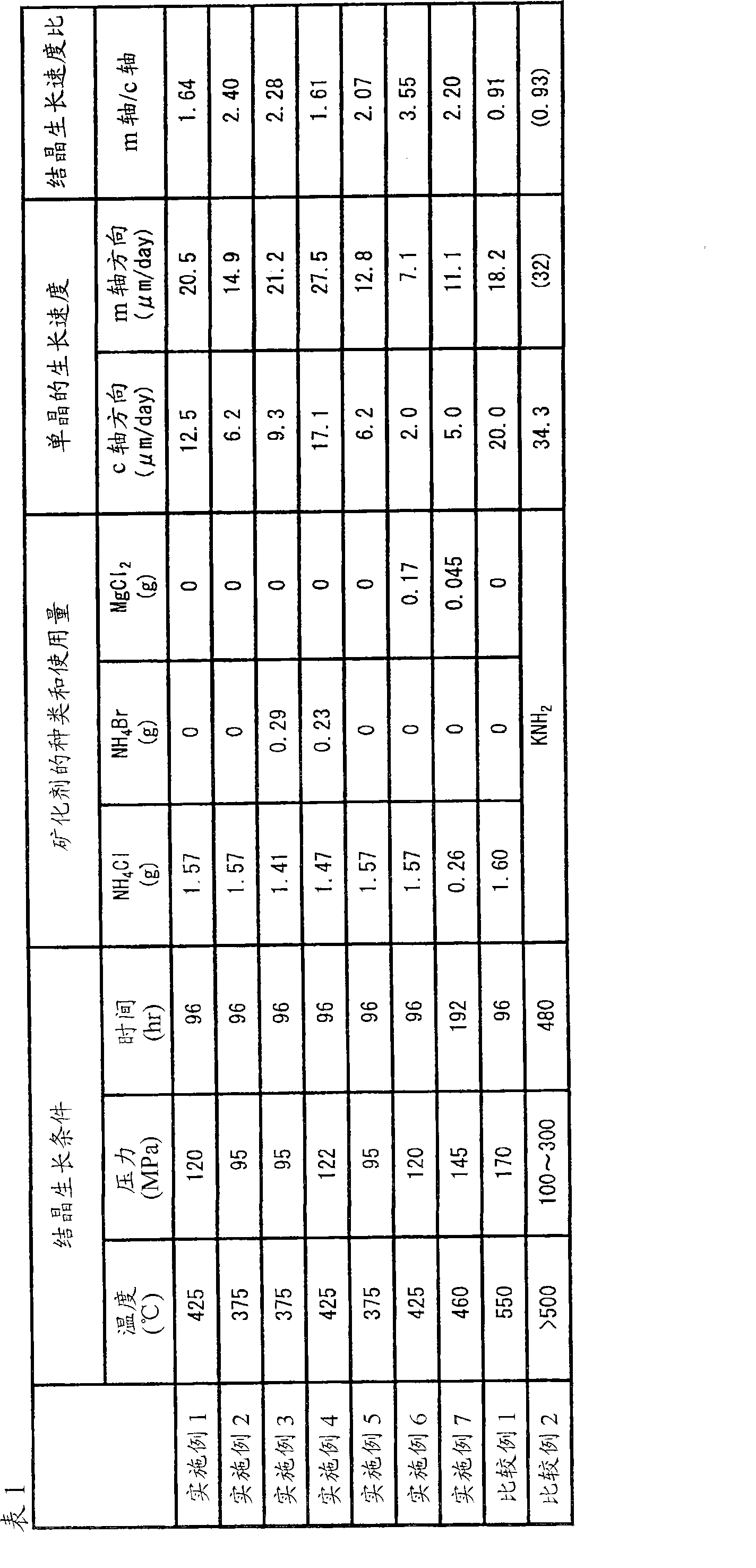
[0132]Except changing the crystal growth conditions of Example 1 and the type and usage amount of the mineralizer as shown in Table 1, the growth of GaN crystals was attempted in the same manner as in Example 1 (Examples 2 to 4, 6, 7 and Comparative Example 1). In Example 5, growth of a GaN crystal was attempted in the same manner as in Example 2, except that a seed crystal having an M-plane produced by slicing instead of cleavage was used. Comparative Example 2 is a technique described in a known document (Journal of Crystal Crowth 287 (2006) 376-380).

[0133] In Examples 2 to 7, the GaN crystal grown on the surface of the seed crystal was taken out and the state of the crystal surface was observed with a SEM (scanning electron microscope). As a result, as in Example 1, no needle crystals and grains were observed. The result of X-ray diffraction measurement is that the crystal shape is hexagonal, and the crystal growth orientation is the same as that of the seed crystal, or...


PUM

PropertyMeasurementUnit
thicknessaaaaaaaaaa

Abstract

This invention relates to a process for producing a nitride semiconductor, comprising the step of regulating the temperature and pressure within an autoclave containing a seed having a crystal structure of a hexagonal system, a nitrogen element-containing solvent, a starting material comprising a metallic element belonging to group 13 of the periodic table, and a mineralizer so that the solvent is brought to a supercritical state and / or a subcritical state to allow a nitride semiconductor crystal to grow ammonothermally on the surface of the seed, wherein the crystal growth rate in m-axis direction on the seed is brought to not less than 1.5 times the crystal growth rate in c-axis direction on the seed. The above constitution can realize the production of nitride semiconductors with a large-diameter c face and nitride semiconductors having a large thickness in m-axis direction in an efficient and simple manner.

Description

technical field [0001] The present invention relates to a method for producing nitride semiconductor crystal growth on a seed crystal by using a solvent in a supercritical state and / or a subcritical state together with a raw material and a mineralizer, and its crystal growth rate In addition, the present invention also relates to nitride single crystals, wafers and devices manufactured by the method. Background technique [0002] Nitride semiconductors represented by gallium nitride (GaN) can be used in light-emitting devices such as light-emitting diodes and laser diodes, or high-frequency and high-output electronic devices such as HEMTs and HBTs. Especially in the application of electronic devices, where there is a prospect of market expansion in the future, the element size is larger than that of light-emitting devices. Therefore, from the viewpoint of productivity, it is strongly desired to further increase the diameter of the wafer. A high degree of uniformity in cryst...

Claims


Application Information

Patent Timeline
Patent Type & Authority Applications(China)
IPC IPC(8): C30B29/38C30B7/10
CPCC30B7/10C30B29/403C30B29/406C30B29/38H01L21/20
Inventor 川端绅一郎伊藤浩久德克·埃伦特劳特镜谷勇二吉川彰福田承生
Owner MITSUBISHI CHEM CORP
Why Eureka
Try Eureka