Thin film transistor and production method thereof

A technology of thin film transistors and manufacturing methods, applied in the direction of transistors, semiconductor/solid-state device manufacturing, electrical components, etc., can solve problems such as limitations, inability to shrink arbitrarily, and inability to effectively improve the control ability of nanoscale channels 118, etc., to achieve good Effect of component properties

Inactive Publication Date: 2009-09-16
CHUNGHWA PICTURE TUBES LTD
View PDF0 Cites 1 Cited by
  • Summary
  • Abstract
  • Description
  • Claims
  • Application Information

AI Technical Summary

Problems solved by technology

It should be noted that since the height of the nanoscale channel 118 mainly depends on the height of the gate 114, the size of the gate 114 is limited and cannot be reduced arbitrarily.
Therefore, the size of the nanoscale channel 118 is directly limited by the size of the gate 114
In addition, since only one side of the nanoscale channel 118 is opposite to the gate 114, the control ability of the gate 114 for the nanoscale channel 118 cannot be effectively improved.

Method used


Image

  • Thin film transistor and production method thereof
  • Thin film transistor and production method thereof
  • Thin film transistor and production method thereof

Examples


no. 1 example

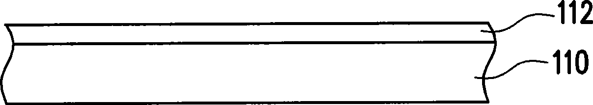
[0052] Figure 2A-2H is a top view of the flow of the manufacturing method of the thin film transistor according to the first embodiment of the present invention, and Figures 3A-3H It is a schematic cross-sectional flow diagram of the manufacturing method of the thin film transistor according to the first embodiment of the present invention. Please refer to Figure 2A and Figure 3A , firstly, a substrate 210 is provided. Generally speaking, a buffer layer 212 can be selectively formed on the substrate 210 to facilitate the fabrication of subsequent film layers. The material of the buffer layer 212 may include silicon oxide, silicon nitride or silicon oxynitride.

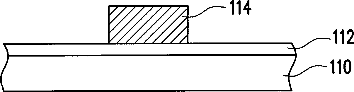
[0053] Then please refer to Figure 2B and Figure 3B , forming a sacrificial layer 220 on the substrate 210 . In detail, the sacrificial layer 220 is formed by, for example, depositing a material layer (not shown) on the buffer layer 212 in an all-round way. The material layer can be made of silicon oxide,...

no. 2 example

[0063] The second embodiment is similar to the first embodiment, and the main difference between the two is that the sacrificial layer is not removed in this embodiment. The initial manufacturing process of the thin film transistor in the second embodiment and Figure 2A ~ Figure 2C as well as Figure 3A ~ Figure 3C The steps shown are the same and will not be repeated here.

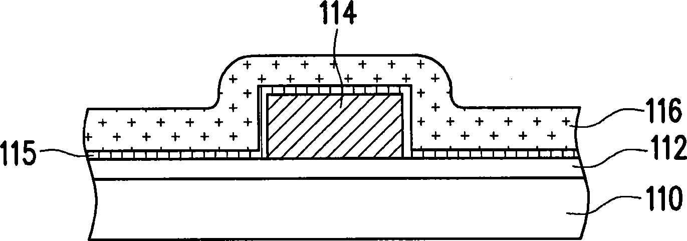
[0064] Then please refer to Figure 4A and Figure 5A , forming a gate insulating layer 240 to cover the polysilicon pattern layer 230 and the sacrificial layer 220 . The gate insulating layer 240 can be made of silicon nitride (SiN) or silicon oxide (SiO) formed by using tetraethoxysilane (TEOS) as a reactive gas source.

[0065] Then please refer to Figure 4B and Figure 5B , forming a gate pattern 250 on the gate insulating layer 240 above the polysilicon pattern layer 230 . The gate pattern 250 is, for example, deposited metal material or polysilicon material on the gate insulating layer 240 ...


PUM


Abstract

The invention discloses a production method of a thin film transistor, which comprises the following steps of: providing a base plate firstly; forming a sacrificial layer on the base plate; forming a multicrystal silicon pattern layer on the base plate to surround the sacrificial layer; and then forming a gate insulation layer large enough to cover the multicrystal silicon pattern layer at least. Additionally, a gate pattern is formed on the gate insulation layer above the multicrystal silicon pattern layer and a source electrode region, a drain electrode region and an active region are formed on the multicrystal silicon pattern layer and the active region is positioned between the source electrode region and the drain electrode region. Furthermore, a protection layer is formed to cover the gate pattern and partial gate insulation layer. And then a source electrode conducting layer and a drain electrode conducting layer are formed on the protection layer and electrically connected with the source electrode region and the drain electrode region of the multicrystal silicon pattern layer respectively.

Description

technical field [0001] The present invention relates to a thin film transistor and its manufacturing method, and in particular to a polysilicon thin film transistor and its manufacturing method. Background technique [0002] In existing low-temperature polysilicon thin film transistors, grain boundary defects in the channel are the main factor for deteriorating device characteristics. Since the size of the channel is reduced to nanoscale, the problem of grain boundary defects in the channel can be effectively improved. Therefore, how to fabricate a nanowire channel (NW channel) has become a major research direction. [0003] The existing nanoscale channel fabrication method mainly utilizes electron beam lithography (electron beamlithography) technology to pattern polysilicon material to form a nanoscale width channel. However, the cost of e-beam lithography is quite high and cannot effectively increase production capacity. Therefore, the technique of fabricating nanoscale...

Claims


Application Information

Patent Timeline
IPC IPC(8): H01L21/336H01L29/786
Inventor 张家文黄俊嘉张子恒雷添福陈司芬
Owner CHUNGHWA PICTURE TUBES LTD
Why Eureka
Try Eureka