Double patterning for lithography to increase feature spatial density

A pattern and spatial frequency technology, applied in the field of density of feature space, can solve problems such as not easy to be compatible with photoresist

Inactive Publication Date: 2009-09-23
NXP BV
View PDF1 Cites 13 Cited by
  • Summary
  • Abstract
  • Description
  • Claims
  • Application Information

AI Technical Summary

Problems solved by technology

This technology is therefore not easily compatible with photoresists

Method used


Image

  • Double patterning for lithography to increase feature spatial density
  • Double patterning for lithography to increase feature spatial density
  • Double patterning for lithography to increase feature spatial density

Examples


Embodiment Construction

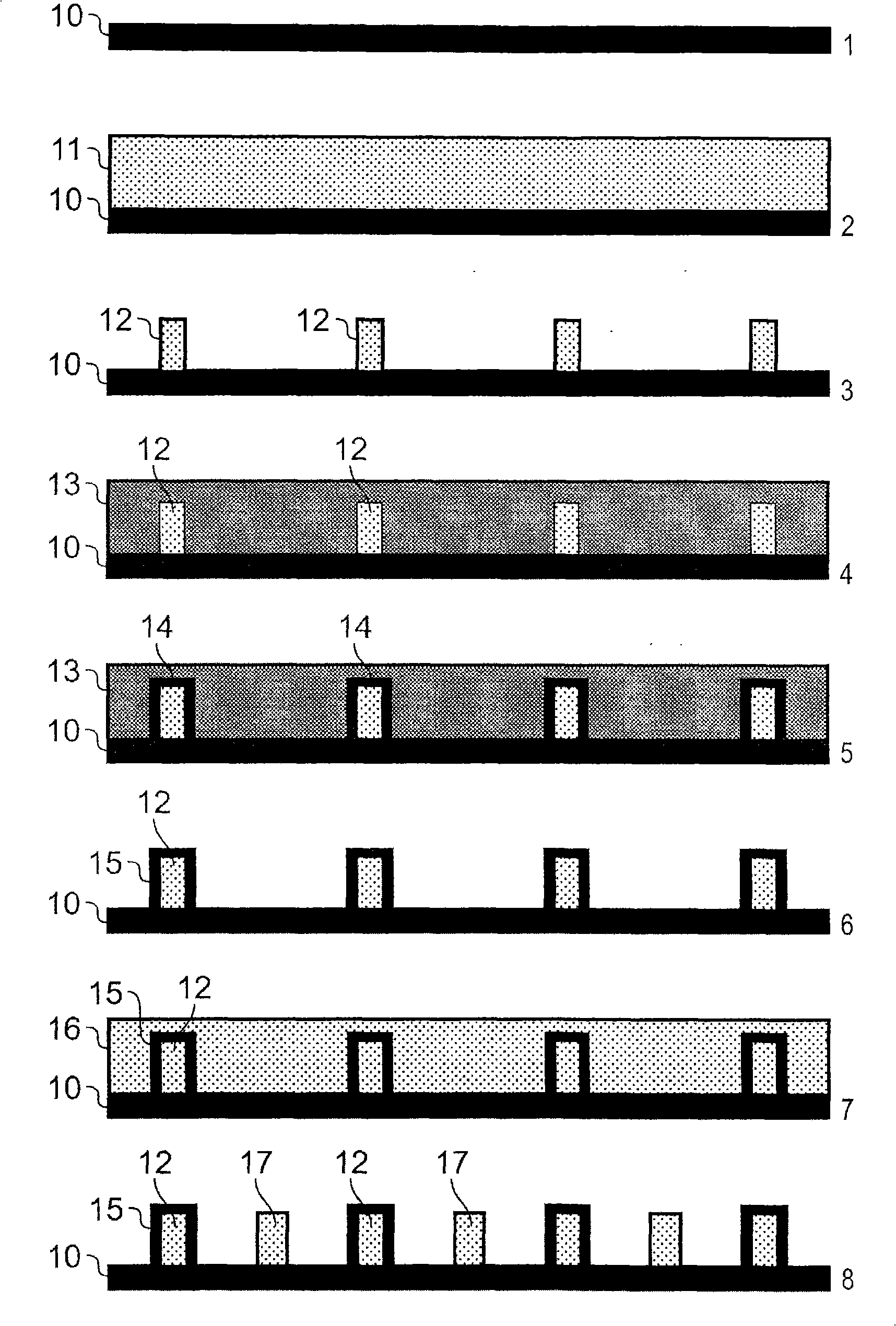
[0032] figure 1 A schematic cross-sectional view representing the process sequence of the two-time patterning technique is provided.

[0033] Picture 1-1 The device layer 10 of the substrate is shown ready for lithographic processing. Throughout the specification, unless expressly stated otherwise, the expression "substrate" does not only denote the original (eg silicon wafer) substrate, but also any subsequently deposited and / or defined layer up to the relevant point in the process being described. therefore, Picture 1-1 The device layer 10 may comprise a base silicon wafer or other semiconductor wafer or other bare substrate suitable for forming an integrated circuit, or an uppermost device layer processed by earlier deposited and / or defined layers, eg, from earlier photolithographic steps.

[0034] Accordingly, it should be understood that the device layer 10 need not be planar, especially if it includes earlier patterned layers or surface features that have not been pl...


PUM


Abstract

A method of forming a pattern in at least one device layer in or on a substrate comprises: coating the device layer with a first photoresist layer; exposing the first photoresist using a first mask; developing the first photoresist layer to form a first pattern on the substrate; coating the substrate with a protection layer; treating the protection layer to cause a change therein where it is in contact with the first photoresist, to render the changed protection layer substantially immune to a subsequent exposure and / or developing step; coating the substrate with a second photoresist layer; exposing the second photoresist layer using a second mask; and developing the second photoresist layer to form a second pattern on the substrate without significantly affecting the first pattern in the first photoresist layer, wherein the first and second patterns together define interspersed features having a spatial frequency greater than that of the features defined in each of the first and second patterns separately. The process has particular utility in defining source, drain and fin features of finFET devices with a smaller feature size than otherwise achievable with the prevailing lithography tools.

Description

technical field [0001] The present invention relates to integrated circuit fabrication, and more particularly to techniques for increasing the density of feature spaces defined using photolithographic techniques. Background technique [0002] To achieve higher device densities in integrated circuit fabrication, photolithographic processes are required to print ever smaller feature sizes and spacing between features. Several methods are known in the art to extend the reach of photolithographic processing to smaller and smaller feature sizes and pitches. [0003] One approach is to reduce the wavelength of the radiation used to expose and pattern the photoresist used to the deep ultraviolet (DUV), extreme ultraviolet (FUV) or extreme ultraviolet (EUV) range. It can be considered that the DUV spectrum refers to the wavelength below 300nm, the FUV spectrum refers to the wavelength below 200nm, and the EUV spectrum refers to the wavelength below 31nm (especially including the wa...

Claims


Application Information

Patent Timeline
IPC IPC(8): G03F7/00G03F7/11
CPCH01L29/785G03F7/11H01L21/0273H01L29/66795H01L21/0271G03F7/0035H01L21/823821H01L29/6681
Inventor 阿尼亚·莫妮克·范利恩霍夫彼得·德克森戴维·范斯滕温克尔马克·范达尔赫尔本·多恩博斯卡斯珀·尤弗尔曼斯
Owner NXP BV
Why Eureka
Try Eureka