Low-dimensional nanophase material high-flexibility assembling chip and application method

A low-dimensional nanotechnology, high flexibility technology, applied in nanotechnology, nanotechnology, nanostructure manufacturing and other directions, can solve the problems of poor flexibility, difficulty in realizing three-dimensional control of a single nanomaterial, complex manufacturing process, etc., and achieve the effect of overcoming complex structure.

Inactive Publication Date: 2009-09-30
SOUTHEAST UNIV
View PDF0 Cites 18 Cited by
  • Summary
  • Abstract
  • Description
  • Claims
  • Application Information

AI Technical Summary

Problems solved by technology

[0011] Technical problem: The purpose of the present invention is to provide a low-dimensional nanostructure material highly flexible assembly chip and its application method, which can manipulate a single low-dimensional nanomaterial in three-dimensional space and complete the assembly, so as to solve the current precision electrode structure used for nanomaterial assembly. Difficult to realize the lack of three-dimensional control of a single nanomaterial, and the defects of complex manufacturing process, high manufacturing cost, and poor flexibility

Method used


Image

  • Low-dimensional nanophase material high-flexibility assembling chip and application method
  • Low-dimensional nanophase material high-flexibility assembling chip and application method
  • Low-dimensional nanophase material high-flexibility assembling chip and application method

Examples


Embodiment Construction

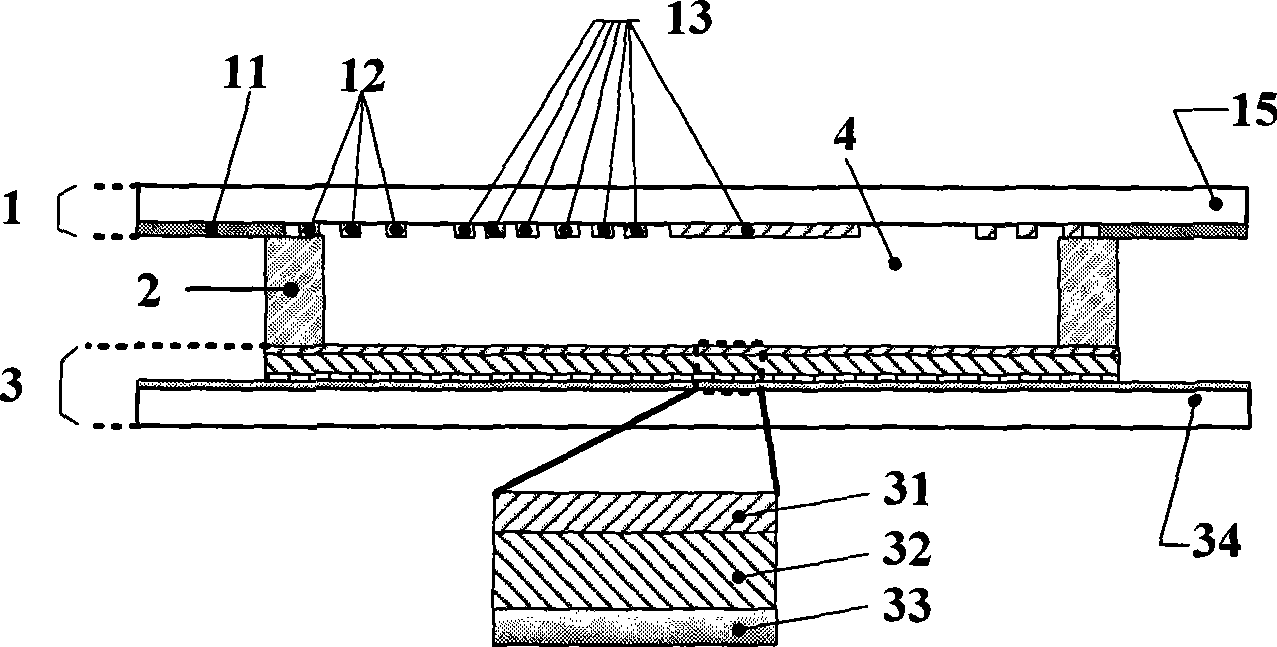
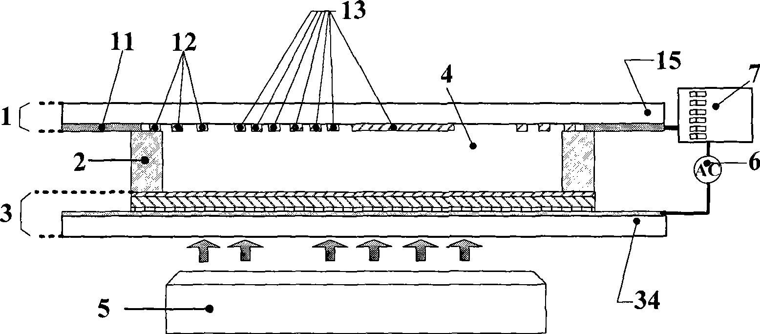
[0029] The embodiment of the highly flexible active assembly chip based on three-dimensional dielectrophoresis low-dimensional nanomaterials provided by the present invention can be found in figure 1 , figure 2 and image 3 . The method of assembling the chip structure, material and configuration of the chip peripheral components is not limited to this embodiment.

[0030] In this embodiment, the structure of the assembly control chip used for nanomaterial assembly is as follows figure 1 shown. The assembled control chip is composed of an upper substrate 1 , a spacer layer 2 and a lower substrate 3 . The microelectrode array 13 , leads 12 and pins 11 are located on the lower surface of the upper substrate 1 and between the upper transparent substrate 15 and the microfluidic chamber 4 . The lower substrate is composed of an insulating layer 31 , a photoconductive layer 32 , an indium tin oxide film 33 and a lower transparent substrate 34 . The microelectrode array 13 exte...


PUM


Abstract

The invention relates to a low-dimensional nanophase material high-flexibility assembling chip and an application method, which belong to the micro-fluidic field and the nano structure material assembly field. The method realizes the electric field distributing control in a micro-fluidic body (4) according to the following two aspects to further generate micro force used for realizing assembly control: one the one hand, the on-off control of pumping signal of each pin in a pin array (11) is controlled to realize that only some microelectrode arrays (13) have electric potential so as to further change the area size of the effective bounding region of the electric field at the top of the chip; and on the other hand, a virtual aurora pattern array is projected on a photoconductive layer (32) by a micro light pattern generator (5) to further limit the electric field boundary at the bottom of the micro-fluidic body (4) in the chip.

Description

technical field [0001] The invention is a three-dimensionally controllable high-flexibility assembly chip technology of low-dimensional nanomaterials, which relates to the field of microfluidic control and the field of assembly of nanostructure materials, especially the field of active assembly of low-dimensional nanomaterials. Background technique [0002] In recent years, with the development of nanomaterial synthesis technology, metal materials, insulating materials and semiconductor materials can be assembled to form new nanostructure materials, which are used in MEMS devices and biomedical devices. Due to the differences in chemical stability and thermal stability of various nanostructured materials, there are great challenges to achieve high-level assembly of heterogeneous nanostructured materials. The currently used assembly method consists of two steps: firstly, various nanostructure materials are synthesized separately; then, a certain micro-manipulation method is u...

Claims


Application Information

Patent Timeline
Patent Type & Authority Applications(China)
IPC IPC(8): B82B1/00B82B3/00
Inventor 易红朱晓璐倪中华
Owner SOUTHEAST UNIV
Why Eureka
Try Eureka