Energy-efficient semiconductor plastic package die

A high-efficiency, energy-saving, plastic-encapsulated mold technology, applied in semiconductor/solid-state device manufacturing, electrical components, circuits, etc., can solve the problems of complex replacement of inserts and ejector pins, waste of materials, and long time required to improve product competitiveness. , Reduce production costs, save energy consumption

Active Publication Date: 2013-01-30
CHENGDU SHANGMING IND
View PDF1 Cites 0 Cited by
  • Summary
  • Abstract
  • Description
  • Claims
  • Application Information

AI Technical Summary

Problems solved by technology

However, this kind of multi-injection head circuit packaging mold for large cakes still has waste materials, and the replacement of inserts and ejector pins is complicated and takes a long time. At the same time, the waste of materials in single-day cylinder injection molding is even more serious.

Method used


Image

  • Energy-efficient semiconductor plastic package die
  • Energy-efficient semiconductor plastic package die
  • Energy-efficient semiconductor plastic package die

Examples


Embodiment 1

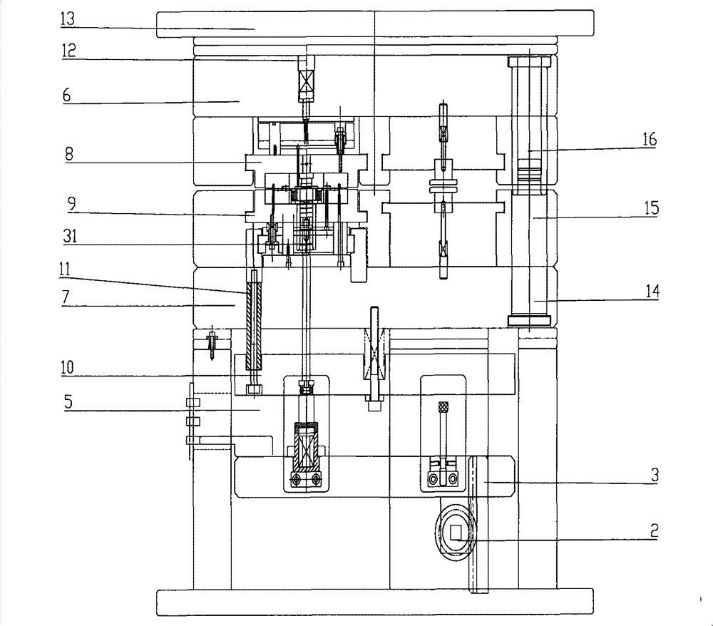
[0020] Such as figure 1 As shown in the multi-cylinder injection molding high-efficiency and energy-saving semiconductor plastic sealing mold, the upper template 6 is fixed with the upper mold box system 8, and the lower template 7 is fixed with the lower mold box 9; the gear rack 2 is connected to the drive transfer plate 3, and reciprocates up and down Move and fix the injection head system on the transfer board 3; the injection head system is connected with the lower center runner plate of the lower mold box 9; The lower mold ejector rod power rod 11 passing through the lower mold plate 7 through the reset rod of the machine tool drives the ejector rod to move upward to eject the molded product and the runner; the upper mold ejector rod reset power system 12 pushes against the upper mold bottom plate 13 and the upper mold box 8, the upper mold ejector rod reset power system 12 drives the upper mold ejector rod to move downward, ejecting the molded product and the runner; af...

Embodiment 2

[0024] Such as figure 1 As shown in the multi-cylinder injection molding high-efficiency and energy-saving semiconductor plastic sealing mold, the upper template 6 is fixed with the upper mold box system 8, and the lower template 7 is fixed with the lower mold box 9; the gear rack 2 is connected to the drive transfer plate 3, and reciprocates up and down Move and fix the injection head system on the transfer board 3; the injection head system is connected with the lower center runner plate of the lower mold box 9; The lower mold ejector rod power rod 11 passing through the lower mold plate 7 through the reset rod of the machine tool drives the ejector rod to move upward to eject the molded product and the runner; the upper mold ejector rod reset power system 12 pushes against the upper mold bottom plate 13 and the upper mold box 8, the upper mold ejector rod reset power system 12 drives the upper mold ejector rod to move downward, ejecting the molded product and the runner; af...


PUM

PropertyMeasurementUnit
diameteraaaaaaaaaa
widthaaaaaaaaaa

Abstract

The invention discloses an energy-efficient semiconductor plastic package die, wherein the upper central casting plate of the upper die box (8) and the lower central casting plate of the lower die box (9) form a closed cavity; the upper die box (8) and the lower die box (9) are provided with gel passages (24) which are hollow pipelines connected with the flow passage (25); the gel passages (24) are connected with an integrated component cavity (26) via the flow passage (25); the casting head (4) is connected with the cavity; the liquid resin of the feeding cylinder (31) is infused via the flow passage and the flow passage (25) by the casting head. The invention overcomes the disadvantages of long casting process of current technology, bad air tightness of plastic-casting products, and complication of insert and mandril exchange. The invention provides a semiconductor plastic package die with large density, convenient disassembly and little plastic package material waste, saves 15%-30% resin, and improves utilization rate of the raw material, which can be applied in the field of IC package.

Description

technical field [0001] The present invention relates to injection molding equipment, in particular to packaging equipment for integrated circuits Background technique [0002] Semiconductor integrated circuit packaging molds are essential key process equipment for microelectronic packaging production. The rapid development of the microelectronics industry has put forward high-level high-tech requirements for the design and manufacture of semiconductor packaging molds. [0003] The requirements of the semiconductor packaging mold industry for molds are: first, the molds are required to be finished. At present, electronic products are continuously integrated and miniaturized, and the products tend to be high-end, and the size is getting smaller and smaller. The higher the value, the higher the precision requirements for the mold. The plastic molding process is one of the most important process means in the post-production process of semiconductor devices. Single-cylinder pack...

Claims


Application Information

Patent Timeline
Patent Type & Authority Patents(China)
IPC IPC(8): B29C45/26B29C45/27B29C45/34H01L21/56
Inventor 刘明华熊蜀宁邹学彬刘翔东袁威
Owner CHENGDU SHANGMING IND
Why Eureka
Try Eureka