Gate associated transistor of trough arsenic-doped polysilicon structure

A technology of combined gate transistors and gate polysilicon, which is applied in the direction of semiconductor devices, electrical components, circuits, etc., can solve the problems of poor resistance to avalanche breakdown, and achieve enhanced ability to resist avalanche breakdown, low cost, and high cost performance. Effect

Inactive Publication Date: 2009-10-07
HANGZHOU UG MIN SEMICON TECH CO LTD
View PDF1 Cites 10 Cited by
  • Summary
  • Abstract
  • Description
  • Claims
  • Application Information

AI Technical Summary

Problems solved by technology

[0007] In the embodiment of prior art 1, the junction depth of the P-type high-concentration trench gate region is 3-6 μm, which belongs to the shallow junction depth, resulting in relatively poor resistance to avalanche breakdown

Method used


Image

  • Gate associated transistor of trough arsenic-doped polysilicon structure
  • Gate associated transistor of trough arsenic-doped polysilicon structure
  • Gate associated transistor of trough arsenic-doped polysilicon structure

Examples


Embodiment Construction

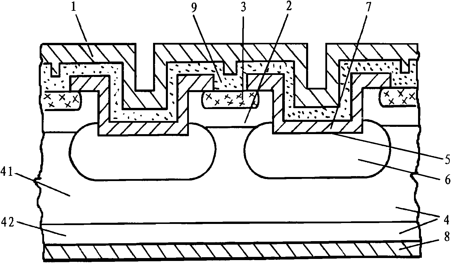
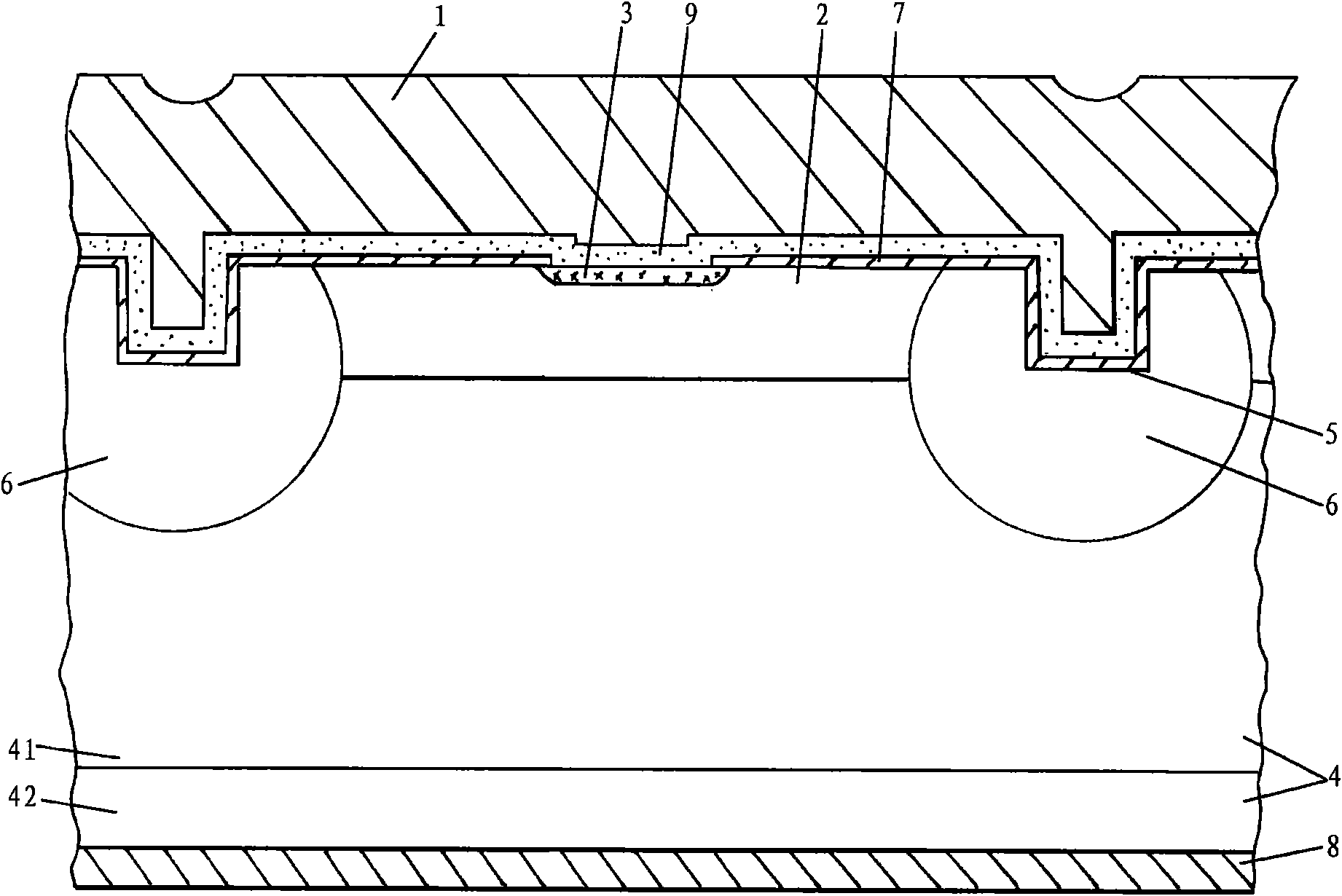
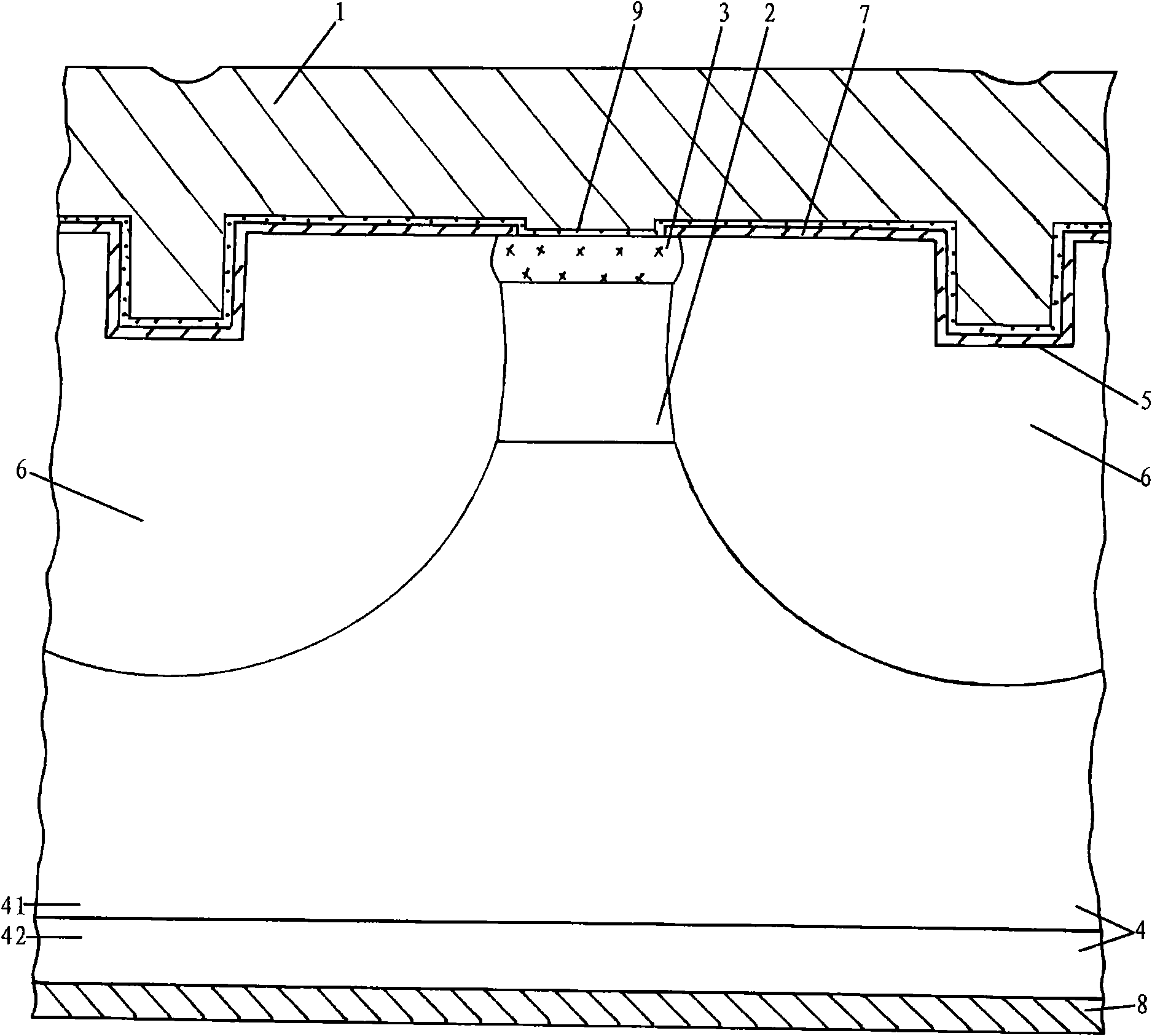
[0020] exist image 3 In the embodiment of the gate transistor with the polysilicon structure of the groove gate shown, the lower layer 42 of the silicon substrate 4 is the collector, which is N-type silicon with a thickness of 420 μm and a resistivity of 0.01 Ω·cm, and the upper layer 41 is a thickness of 60 μm. 35Ω·cm N-type silicon. A plurality of parallel elongated grooves 5 are formed on the upper surface of the silicon substrate 4, the distance between two adjacent grooves 5 is 20 μm, and the depth of the grooves 5 is 3 μm. The bottom of the groove is implanted with boron ions and pushed forward to form a P-type high-concentration groove-shaped gate region 6, and the surface concentration of boron is IE19-2E20 / cm 3 , a junction depth of 10 μm. The upper surface of the upper layer 41 of the silicon substrate is implanted and diffused with boron ions to form a P-type base region 2, and the surface concentration of boron in the P-type base region 2 is 1E17-3E18 / cm 3 , a ...


PUM


Abstract

The invention relates to a gate associated transistor of a trough arsenic-doped polysilicon structure, a plurality of N-type high doping concentration emitting regions are arranged on the upper surface of a silicon substrate wafer, the lower layer of the silicon substrate wafer is an N-type low resistivity layer, the upper layer thereof is an N-type high resistivity layer, and a doped polysilicon layer is connected on tops of the emitting regions. The gate associated transistor is characterized in that an impurity source for doping the polysilicon is arsenic, and the thickness of the doped polysilicon is 0.01-0.30 mu m. The gate associated transistor has the advantages that the anti-avalanche breakdown ability is enhanced, the failure rate in applications is reduced by two orders of magnitude and the gate associated transistor has significant effects of low cost and high performance-price ratio.

Description

technical field [0001] The invention relates to a connected gate transistor, which belongs to the technical field of silicon semiconductor devices. Background technique [0002] In 1979, Hisao Kondo proposed the gate associated transistor GAT (Gate Associated Transistor), followed by a detailed analysis (see IEEE Trans. Electron Device, vol. ED-27, PP.373-379.1980). In 1994, Chen Fuyuan, Jin Wenxin, and Wu Zhonglong made a further analysis of the gate transistor GAT (see "Power Electronics Technology", No. 4, 1994, 1994.11.pp52-55), pointing out that the gate transistor device exhibits high withstand voltage, Excellent characteristics such as fast switching and low saturation voltage drop. [0003] The early connected-gate transistors GAT all adopt planar structure. In 2000, Chinese invention patent ZL00100761.0 (hereinafter referred to as prior art 1) proposed a multi-gate transistor with a groove gate polysilicon structure, and the principle of its structure is as follow...

Claims


Application Information

Patent Timeline
Patent Type & Authority Applications(China)
IPC IPC(8): H01L29/739H01L29/423H01L29/49
Inventor 李思敏
Owner HANGZHOU UG MIN SEMICON TECH CO LTD
Why Eureka
Try Eureka