Circuit base plate and manufacturing method thereof

A technology of circuit substrate and manufacturing method, which is applied in the direction of printed circuit manufacturing, printed circuit, printed circuit, etc., can solve the problems of large difference in expansion and shrinkage, easy peeling of conductive lines and substrates, warping of circuit board products, etc. Achieve the effects of avoiding impact, good electrical conduction, and not easy to warp

Active Publication Date: 2009-10-07
AVARY HLDG (SHENZHEN) CO LTD +1
View PDF3 Cites 6 Cited by
  • Summary
  • Abstract
  • Description
  • Claims
  • Application Information

AI Technical Summary

Problems solved by technology

After heating, different degrees of expansion and contraction occur between the conductive circuit and the base material, and the degree of expansion and contraction is quite different, which makes the conductive circuit and the base material easy to peel off, causing the final circuit board product to warp

Method used


Image

  • Circuit base plate and manufacturing method thereof
  • Circuit base plate and manufacturing method thereof
  • Circuit base plate and manufacturing method thereof

Examples


Embodiment Construction

[0012] The circuit substrate and the manufacturing method of the circuit substrate provided by the embodiment of the technical solution will be further described in detail below with reference to the drawings and embodiments.

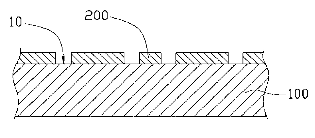
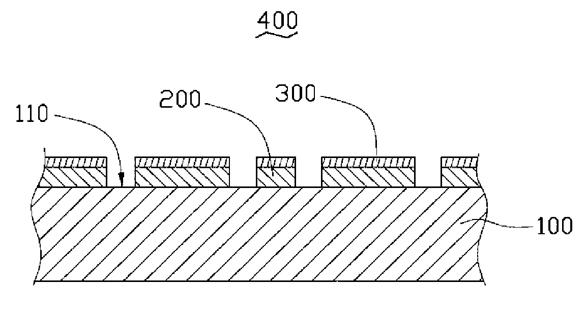
[0013] see Figure 1 to Figure 3 , the circuit substrate and the manufacturing method of the circuit substrate provided in this embodiment.

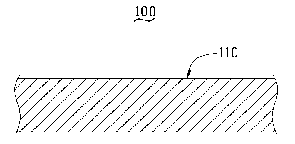
[0014] Step 1: providing a substrate 100 .

[0015] Such as figure 1 As shown, in this embodiment, the base material 100 is a semi-finished product that needs to be circuit-fabricated. The base material 100 with different structures can be selected as required. For example, the substrate 100 can be an insulating layer, and the insulating layer can be made of polyimide, polyester, liquid crystal polymer and other insulating materials. The base material 100 may also be a composite structure formed by laminating a multilayer circuit board and an insulating layer. In addition, the substrate 100 can also be a semi...


PUM

PropertyMeasurementUnit
particle diameteraaaaaaaaaa
lengthaaaaaaaaaa
particle diameteraaaaaaaaaa

Abstract

The invention provides a circuit base plate which comprises base materials and a conductive circuit formed on the surface of the base plate, wherein the conductive circuit comprises a compound of a carbon nano tube and metal nano-particles as well as a metal plated on the surface of the compound. The plating metal is filled in a clearance between two adjacent metal nano-particles so as to cause the two metal nano-particles to be completely combined by the metal, thus realizing good electric conduction. The invention also provides a manufacturing method of the circuit base plate. The circuit base plate has good conductivity, and the difference of expanding and shrinkage degree between the conductive circuit and the base materials is reduced.

Description

technical field [0001] The invention relates to the technical field of inkjet printing, in particular to a circuit substrate and a method for manufacturing the circuit substrate. Background technique [0002] As a printing process, inkjet printing (also called: inkjet printing) can be used for graphic transfer just like lithographic printing and screen printing. Inkjet printing is a non-contact printing process. It does not need to print the surface like movable type and printing plates or films made by photographic methods. It only needs to directly give the required graphics by the computer, and then control the nozzles of the inkjet printing system through the controller. , the ink particles are ejected from the nozzle and form graphics point by point. Inkjet printing can be applied in the production of circuit board circuits, that is, inkjet printed circuit graphics. The method for producing circuit graphics can accurately control the position and width of the circuit,...

Claims


Application Information

Patent Timeline
Patent Type & Authority Applications(China)
IPC IPC(8): H05K1/09H05K3/12C09D11/00
CPCH05K3/125H05K2201/0323H05K3/246H05K2201/026B82Y10/00H05K1/097H05K2201/0272H05K2201/0347H05K2203/013Y10T29/49155Y10T428/2462Y10T428/30Y10T428/32
Inventor 刘兴泽白耀文林承贤
Owner AVARY HLDG (SHENZHEN) CO LTD
Why Eureka
Try Eureka