Shift register and grid drive set of liquid crystal display

A shift register and gate technology, applied in static memory, static indicator, digital memory information and other directions, can solve the problems of threshold voltage shift, reduce the reliability of the shift register, affect the life of the shift register, etc. The effect of outputting noise and ensuring normal working life

Active Publication Date: 2009-10-14
BOE TECH GRP CO LTD +1
View PDF0 Cites 44 Cited by
  • Summary
  • Abstract
  • Description
  • Claims
  • Application Information

AI Technical Summary

Problems solved by technology

If there are a total of 1000 rows of liquid crystal pixels, and one shift register controls a row of thin film transistors, each shift register is only in the working state for T / 1000 of the time T / 1000 of the time when the liquid crystal display displays a frame of image, and most of the rest of the time In the non-working state, the transistors T202 and T204 are biased by almost DC, which will cause a large threshold voltage shift of T202 and T204, which reduces the reliability of the shift register and will eventually affect the shift register. life

Method used


Image

  • Shift register and grid drive set of liquid crystal display
  • Shift register and grid drive set of liquid crystal display
  • Shift register and grid drive set of liquid crystal display

Examples


Embodiment Construction

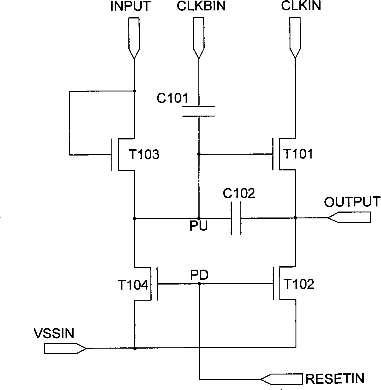
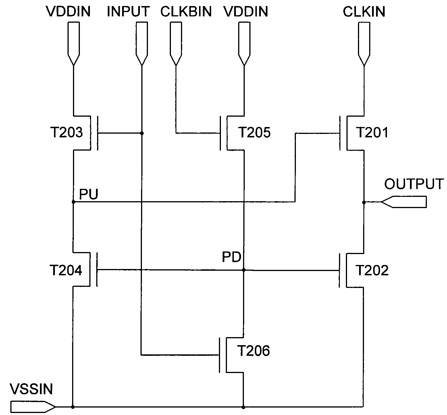
[0061] Such as Figure 5 Shown is a schematic structural diagram of a shift register embodiment of the present invention, the shift register includes: thin film transistors T301, T302, T303, T304, T111, T112, a first pull-down thin film transistor driving unit 1 and a second pull-down thin film transistor driving unit In unit 2, the drain of T301 is connected to the first clock signal input terminal (CLKIN), the gate is connected to the first pull-down thin film transistor drive unit 1 and one end of capacitor C301, and the source is connected to the other end of C301 and the signal output terminal (OUTPUT); the drain of T302 is connected to the source of T301, the gate is connected to the reset signal input terminal (RESETIN), and the source is connected to the low voltage signal input terminal (VSSIN); the drain of T303 is connected to the high voltage signal The input terminal (VDDIN) is connected, the gate is connected to the input signal terminal (INPUT); the drain of T30...


PUM


Abstract

The invention relates to a shift register and a grid driver set of a liquid crystal display. The shift register comprises a first thin film transistor, a second thin film transistor, a third thin film transistor, a fourth thin film transistor, a first pull-down thin film transistor, a second pull-down thin film transistor, a first pull-down thin film transistor drive unit and a second pull-down thin film transistor drive unit, wherein the first pull-down thin film transistor drive unit is used for controlling the first pull-down thin film transistor to open when a signal output end outputs a low level and a first clock signal input end inputs a high level; and the second pull-down thin film transistor drive unit is used for controlling the second pull-down thin film transistor to open when the signal output end outputs a low level and a second clock signal input end inputs a high level. The shift register and the grid drive set of a liquid crystal display can effectively restrain output noise and can ensure that the shift register and each thin film transistor in the grid drive set can not generate great threshold voltage excursion, thereby ensuring the normal service life of the shift register and the grid drive set.

Description

technical field [0001] The invention relates to the field of liquid crystal display, in particular to a shift register and a gate driving device of a liquid crystal display. Background technique [0002] In the existing shift register, the typical structure is Thomson's four-transistor two-capacitor structure, figure 1 Shown is a schematic diagram of the structure of Thomson's four-transistor two-capacitance shift register. figure 2 shown as figure 1 The input and output timing diagram of the shift register shown, the specific principle is: select figure 2 Part of the timing diagram shown and divided into five stages, in the first stage, the signal input terminal (INPUT) input signal is high level, the reset signal input terminal (RESETIN) input signal is low level, transistor T103 It is turned on, and the transistor T104 is cut off, so the charging of the node PU through the transistor T103 is also high level; in the second stage, the input signal of the signal input t...

Claims


Application Information

Patent Timeline
Patent Type & Authority Applications(China)
IPC IPC(8): G11C19/28G09G3/36
Inventor 商广良
Owner BOE TECH GRP CO LTD
Why Eureka
Try Eureka