
Dual-bus visual processing chip architecture

A visual processing, dual-bus technology, applied in image data processing, image data processing, instruments, etc., can solve the problems of poor scalability, insufficient memory bandwidth, low average communication efficiency, etc., and achieve the effect of perfect synchronization function

Inactive Publication Date: 2009-10-28
XI AN JIAOTONG UNIV
View PDF0 Cites 7 Cited by
  • Summary
  • Abstract
  • Description
  • Claims
  • Application Information

AI Technical Summary

Problems solved by technology

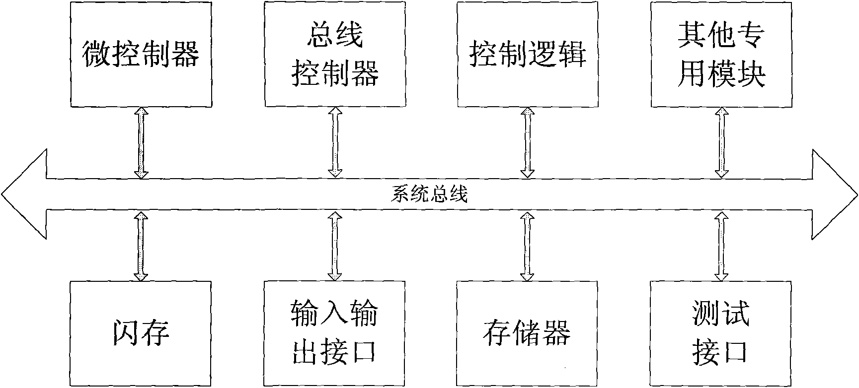
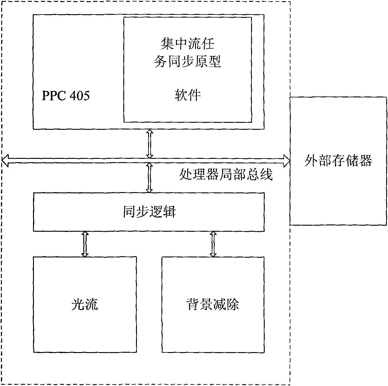
[0004] To sum up, the current vision processing chip structure mainly has the following problems: insufficient memory bandwidth, poor scalability, low average communication efficiency, single clock, etc., which cannot well meet the requirements of actual vision processing

Method used


Image

  • Dual-bus visual processing chip architecture
  • Dual-bus visual processing chip architecture
  • Dual-bus visual processing chip architecture

Examples


Embodiment Construction

[0023] The present invention will be described in detail below in conjunction with the accompanying drawings and specific embodiments.

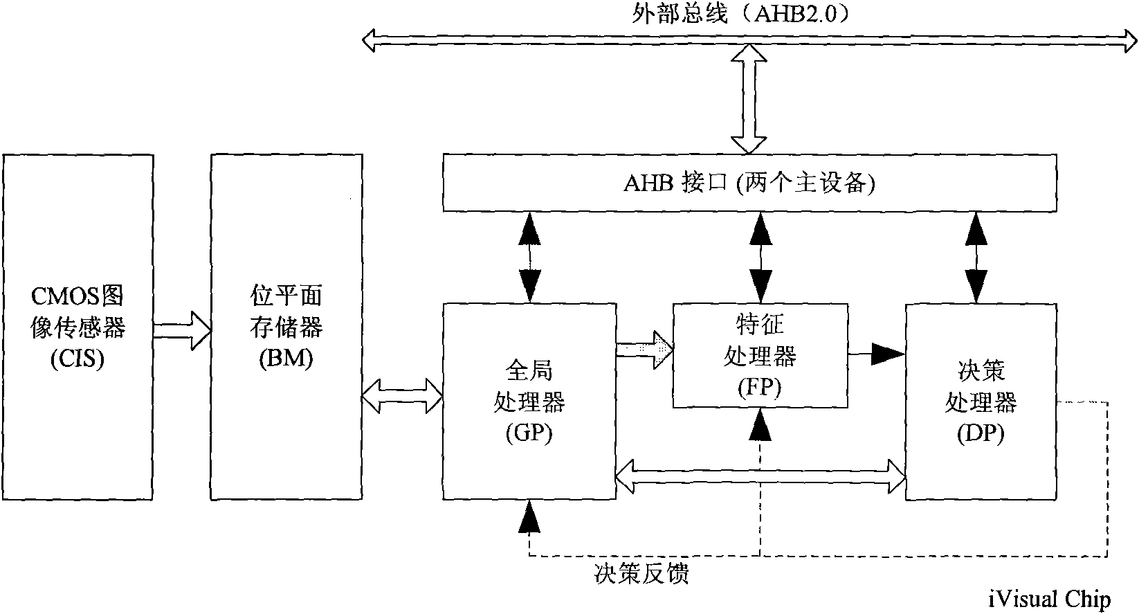
[0024] refer to Figure 4 , the visual processing chip architecture of the dual bus of the present invention mainly includes: a first bus, a second bus, a visual calculation and decision module connected on the first bus, a first memory connected on the first bus, a first memory connected on the second bus, A feature combination and pattern generation module on the bus, an image feature extraction module connected to the second bus, a second memory connected to the second bus, and a bridge circuit connected to the first bus and the second bus.

[0025] The image feature extraction module performs correction and filtering, feature map extraction, down-sampling and non-uniform sampling on video signals, and completes the underlying processing in visual processing. The feature combination and pattern generation module calculates and recombines ...


PUM


Abstract

The invention relates to the field of structural design of visual information processing chips in integrated circuits, and discloses dual-bus visual processing chip architecture. The architecture comprises a first bus, a second bus, a visual computing and deciding module connected to the first bus, a first memory connected to the first bus, a characteristic combination and mode generating module connected to the second bus, an image characteristic extraction module connected to the second bus, a second memory connected to the second bus, and a bridge circuit for connecting the first bus and the second bus.

Description

technical field [0001] The invention relates to the field of structural design of visual information processing chips in integrated circuits, in particular to a dual-bus visual processing chip architecture. Background technique [0002] With the development of large-scale integrated circuit design, System on a Chip (SoC) technology emerges as the times require. IP core (Intellectual Property, IP) multiplexing is an important way to realize SoC. Among them, the on-chip bus is the key technology of IP core interconnection. Its proposal effectively solves the problems of IP core transplantation reuse and system design verification. For vision processing chips, how to combine machine vision with small-volume, low-power-consumption hardware systems to design vision chips with visual perception and image processing functions is currently a research hotspot in the field of vision and intelligent information processing. [0003] According to the characteristics of vision processi...

Claims


Application Information

Patent Timeline
IPC IPC(8): G06T1/00
Inventor 梅魁志张斌郭青赵晨刘传银李宇海雷浩
Owner XI AN JIAOTONG UNIV
Learn More