

Density conversion method and density conversion device for PCB test machine
A conversion device and density conversion technology, applied in the direction of measuring devices, coupling devices, electronic circuit testing, etc., can solve the problems of enterprise failure, small solder joints, dense density, etc., and achieve the effect of eliminating gaps and good electrical connections
- Summary
- Abstract
- Description
- Claims
- Application Information
AI Technical Summary
Problems solved by technology
Method used
Image

Examples
Embodiment Construction
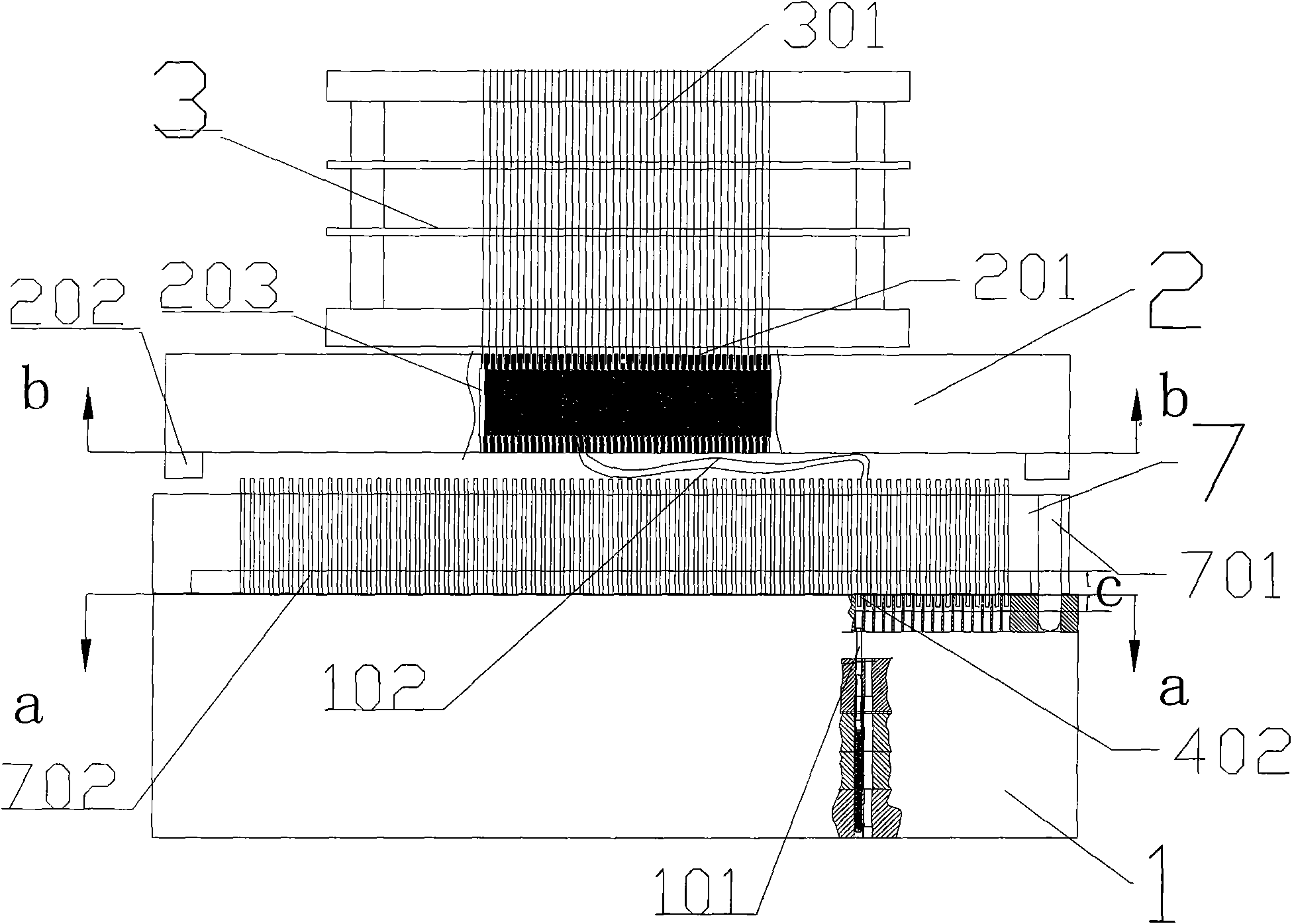
[0018] A density conversion method for a PCB testing machine, by setting a conversion device between the test fixture and the needle bed of the test machine, the device includes a two-layer structure, the upper layer is a conversion needle plate, and the lower layer is a needle row; the upper end of the conversion needle plate corresponds to the test The fixture probe is provided with a mesh contact, and the lower end is provided with a lead wire corresponding to the upper end contact. There is an electrical connection between the contact and the lead wire, and a reset connection is provided under the contact to ensure a good electrical connection between the contact and the test fixture probe. mechanism, while the other end of the lead wire is connected to the lower pin header, which is used to connect the lead wire to the needle bed probe of the test machine and ensure a good electrical connection between them.
[0019] A conversion device suitable for the density conversion ...
PUM
 Abstract
Description
Claims
Application Information