Test structure of breakdown voltage, analytic procedure applying same and wafer

A technology of breakdown voltage and test structure, which is applied in the field of reliability testing of semiconductor technology, can solve problems such as uneven distribution of dielectric breakdown voltage between layers, and achieve the effect of easy and simple implementation

Inactive Publication Date: 2011-08-24
SEMICONDUCTOR MANUFACTURING INTERNATIONAL (BEIJING) CORP
View PDF1 Cites 1 Cited by
  • Summary
  • Abstract
  • Description
  • Claims
  • Application Information

AI Technical Summary

Problems solved by technology

However, there is currently no method that can analyze the uneven breakdown voltage distribution of the interlayer dielectric caused by the above-mentioned reasons.

Method used


Image

  • Test structure of breakdown voltage, analytic procedure applying same and wafer
  • Test structure of breakdown voltage, analytic procedure applying same and wafer
  • Test structure of breakdown voltage, analytic procedure applying same and wafer

Examples


Embodiment Construction

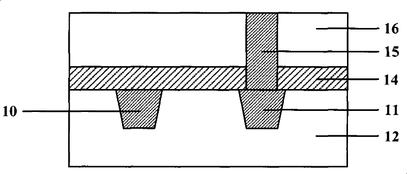
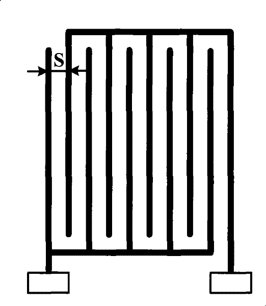
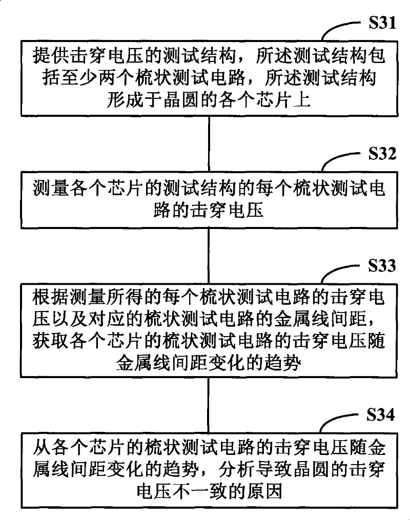
[0028] The breakdown voltage test structure provided by the embodiment of the present invention includes at least two comb-shaped test circuits of metal interconnection lines, wherein the distance between the metal lines in each comb-shaped test circuit is equal, and the metal lines of each comb-shaped test circuit The distances are not equal to each other, and the distance between the metal lines is the distance between any two adjacent metal lines in the comb test circuit. In the embodiment of the present invention, by adding comb-shaped test circuits with different metal line spacings, and measuring the breakdown voltage of each comb-shaped test circuit, it can be analyzed from the trend of the breakdown voltage changing with the metal line spacing that the distribution of the breakdown voltage is different. uniform cause. The specific implementation manners of the present invention will be described in detail below in conjunction with the drawings and embodiments.

[0029...


PUM


Abstract

The invention discloses a test structure of breakdown voltage, an analytic procedure applying the same and a wafer. The test structure comprises at two comb test circuits with metal connection wires, wherein the distances among metal wires in each comb test circuit are equal, the distances among metal wires of the comb test circuits are not equal, and the distances of the metal wires are the distance between any two adjacent metal wires in the comb test circuits. The analytic procedure comprises the following steps: measuring breakdown voltage of each comb test circuit of a test structure of each chip formed on the wafer; obtaining the change trend of breakdown voltage of each comb test circuit of the each chip along with the distance change among the metal wires; and analyzing the reasonof uneven distribution of breakdown voltage of the wafer according to the change trend of breakdown voltage of each comb test circuit of each chip along with the distance change among the metal wires.The invention can quickly analyze the reason of uneven distribution of breakdown voltage of interlamination media of the wafer.

Description

technical field [0001] The invention relates to the reliability test of the semiconductor process, in particular to a breakdown voltage test structure, an analysis method using the test structure and a wafer. Background technique [0002] With the increase of circuit integration, a single metal layer is no longer able to complete the wiring of integrated circuits (IC, Integrated Circuit), but it is necessary to use a multi-layer metal interconnection structure (Multi-layered structure), and, between metal layers requires Separate them with dielectric materials with good insulating properties to prevent short circuits. [0003] figure 1 It is a cross-sectional view of a multilayer copper metal interconnection structure, the lower copper metal lines 10, 11 are isolated by the first dielectric layer 12; the etching barrier layer 14 and the second dielectric layer on the copper metal lines 10, 11 16 are collectively referred to as inter-and intra-layer dielectric (ILD, inter-a...

Claims


Application Information

Patent Timeline
Patent Type & Authority Patents(China)
IPC IPC(8): H01L23/544H01L21/66
CPCH01L2924/0002
Inventor 甘正浩吴永坚
Owner SEMICONDUCTOR MANUFACTURING INTERNATIONAL (BEIJING) CORP
Why Eureka
Try Eureka