Solid-state imaging device and electronic device

A technology of solid-state imaging devices and pixels, which is applied in the direction of electric solid-state devices, semiconductor devices, radiation control devices, etc., and can solve the problems of low blue sensitivity

Inactive Publication Date: 2009-11-18
SONY CORP
View PDF6 Cites 14 Cited by
  • Summary
  • Abstract
  • Description
  • Claims
  • Application Information

AI Technical Summary

Problems solved by technology

Since the silicon nitride film absorbs light with a blue wavelength range of 400nm to 500nm, the blue sensitivity of the silicon nitride film is lower than the red sensitivity and green sensitivity of the silicon nitride film

Method used


Image

  • Solid-state imaging device and electronic device
  • Solid-state imaging device and electronic device
  • Solid-state imaging device and electronic device

Examples


Embodiment Construction

[0043] Embodiments of the present invention will be described below with reference to the drawings.

[0044] The solid-state imaging device according to the embodiment of the present invention and its modification can be applied to a CMOS solid-state imaging device and a CCD solid-state imaging device.

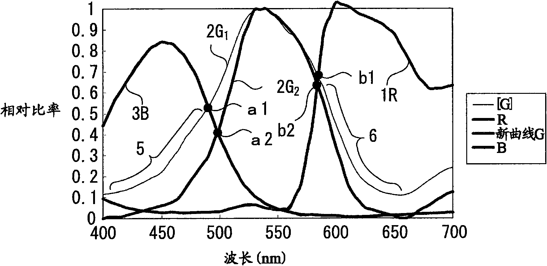
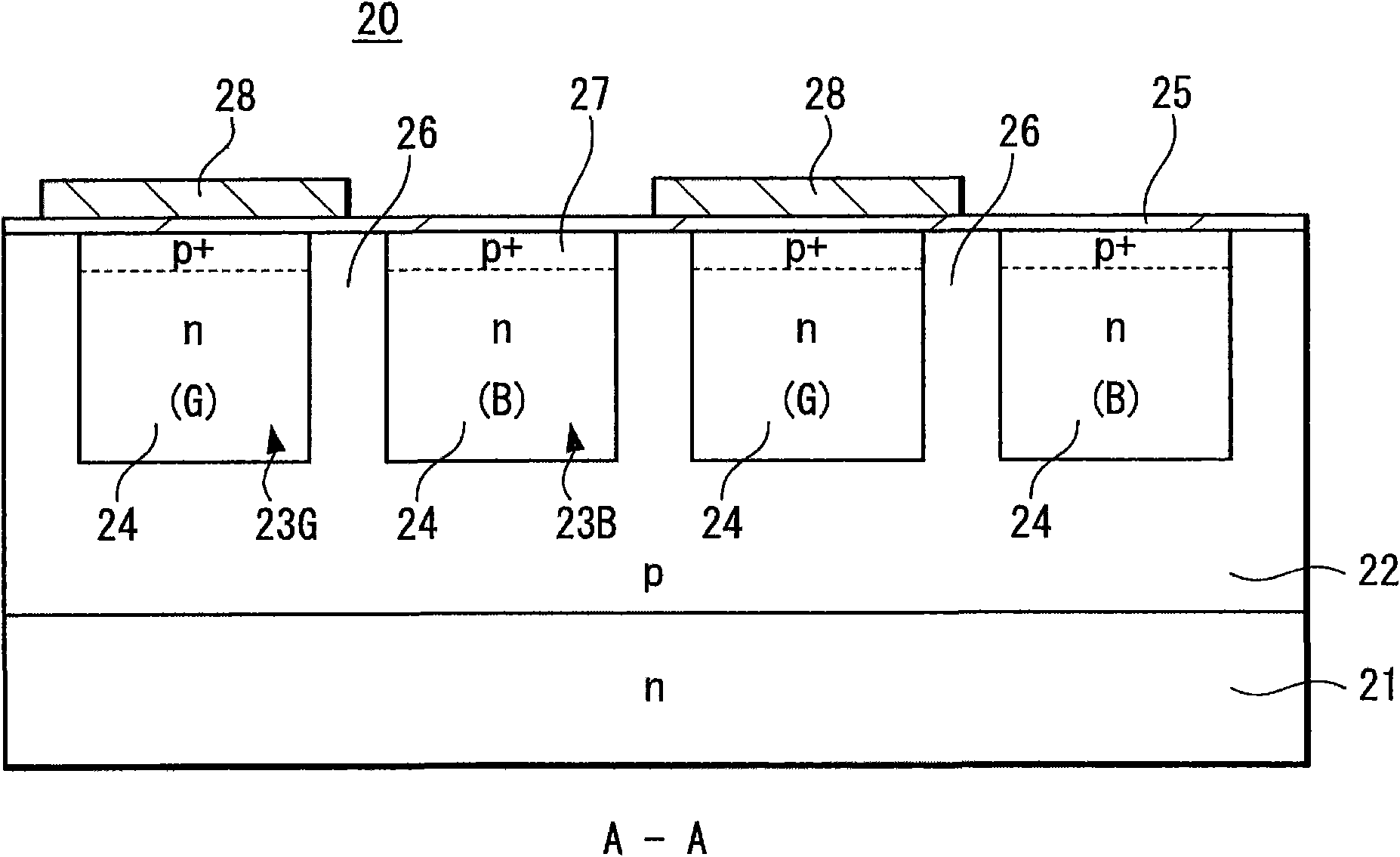
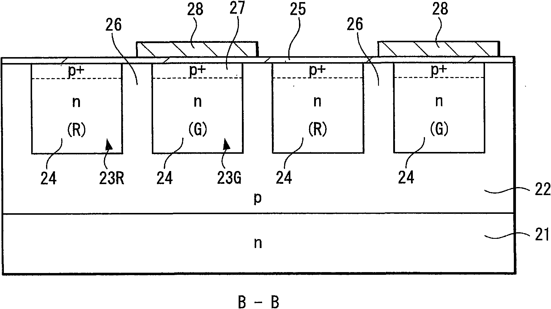
[0045] A general structure of a CMOS solid-state imaging device according to an embodiment of the present invention will be described below. The CMOS solid-state imaging device includes a semiconductor substrate, an imaging region in which a plurality of pixels are two-dimensionally arranged on the semiconductor substrate such as a silicon substrate, and a peripheral circuit section. Each pixel is composed of a photoelectric conversion unit capable of sensing light and generating signal charges, and a plurality of pixel transistors (so-called MOS transistors). The pixel transistor can be composed of four transistors, for example, a transfer transistor, a reset transistor, an ...


PUM


Abstract

The invention discloses a solid-state imaging device and an electronic device. The solid-state image device has pixels in which an absorption film that absorbs short wavelength-side light is formed on a photoelectric conversion portion for desired color light through an insulation film. In the solid-state imaging device, the absorption film absorbs light of short wavelength side of desired color light in the photoelectric conversion portion, therefore floating section of short wavelength side of spectral response curve is reduced. Colour mixture (interference between pixels) namely colour noise is reduced when peak value sensitivity is not reduced. In the electronic device of the solid-state imaging device, colour mixture (interference between pixels) in the photoelectric conversion portion is reduced, thereby image quality is improved.

Description

[0001] Cross References to Related Applications [0002] The present application contains subject matter related to the disclosure of Japanese Priority Patent Application JP 2008-126320 filed in the Japan Patent Office on May 13, 2008, the entire content of which is hereby incorporated by reference. technical field [0003] The present invention relates to solid-state imaging devices such as CMOS image sensors and CCD image sensors, and also to electronic devices such as cameras having such solid-state imaging devices. Background technique [0004] Solid-state imaging devices are classified into amplification-type solid-state imaging devices typified by CMOS image sensors and charge-transport solid-state imaging devices typified by CCD image sensors. When a CMOS image sensor is compared with a CCD image sensor, a higher voltage is applied to the CCD image sensor than to the CMOS image sensor because the CCD image sensor must transmit signal charges using a higher voltage tha...

Claims


Application Information

Patent Timeline
Patent Type & Authority Applications(China)
IPC IPC(8): H01L27/146H04N5/335H04N5/225H01L31/10H04N5/369
CPCH01L27/14603H01L27/14621H01L27/14645H01L27/146
Inventor 糸长总一郎
Owner SONY CORP
Why Eureka
Try Eureka