Alignment signal processing method in photoetching technology

A lithography technology and processing method technology, applied in the field of alignment signal processing, can solve problems such as low power, inability to utilize high-order signals, and inability to reliably provide the highest alignment accuracy

Active Publication Date: 2009-11-25
SHANGHAI MICRO ELECTRONICS EQUIP (GRP) CO LTD
View PDF2 Cites 19 Cited by
  • Summary
  • Abstract
  • Description
  • Claims
  • Application Information

AI Technical Summary

Problems solved by technology

The advantage of this scheme is that it can achieve automatic capture and high alignment accuracy, but the disadvantage is that it requires a special wedge adjustment device and complicated adjustment. In addition, the high-order signals in the diffracted light are weak, while this method is Higher alignment ac

Method used


Image

  • Alignment signal processing method in photoetching technology
  • Alignment signal processing method in photoetching technology
  • Alignment signal processing method in photoetching technology

Examples


Embodiment Construction

[0026] Embodiments of the present invention are described below through specific examples, and those skilled in the art can easily understand other advantages and effects of the present invention from the content disclosed in this specification. The present invention can also be implemented or applied through other different specific examples, and various modifications and changes can be made to the details in this specification based on different viewpoints and applications without departing from the spirit of the present invention.

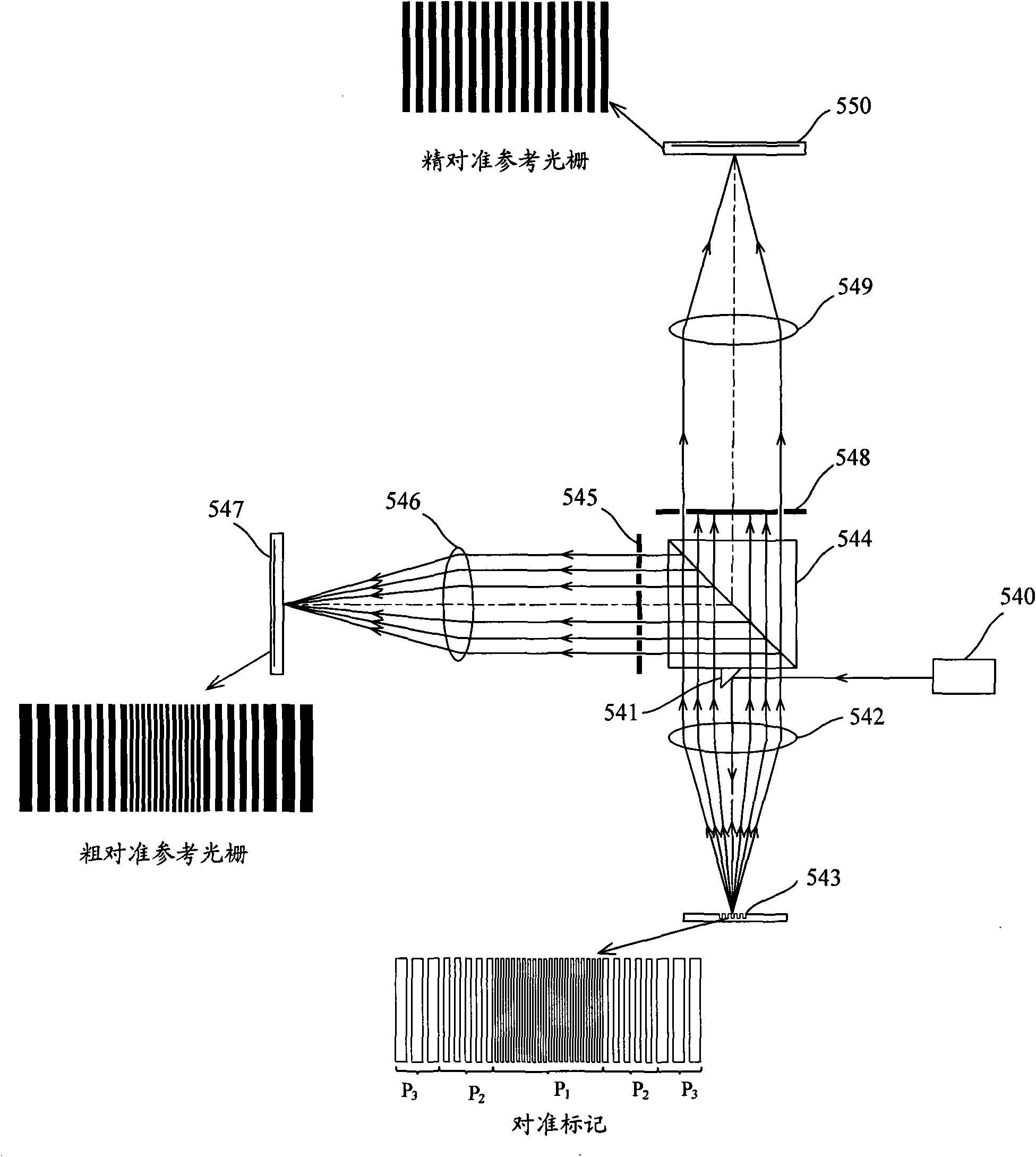
[0027] The specific implementation of the present invention will be further described below in conjunction with the accompanying drawings. It should be noted that the present invention is based on the alignment signals generated by the alignment marks published in Chinese patents 2007100455793 and 2007100455806. Standard marks and related technologies will not be described in detail here.

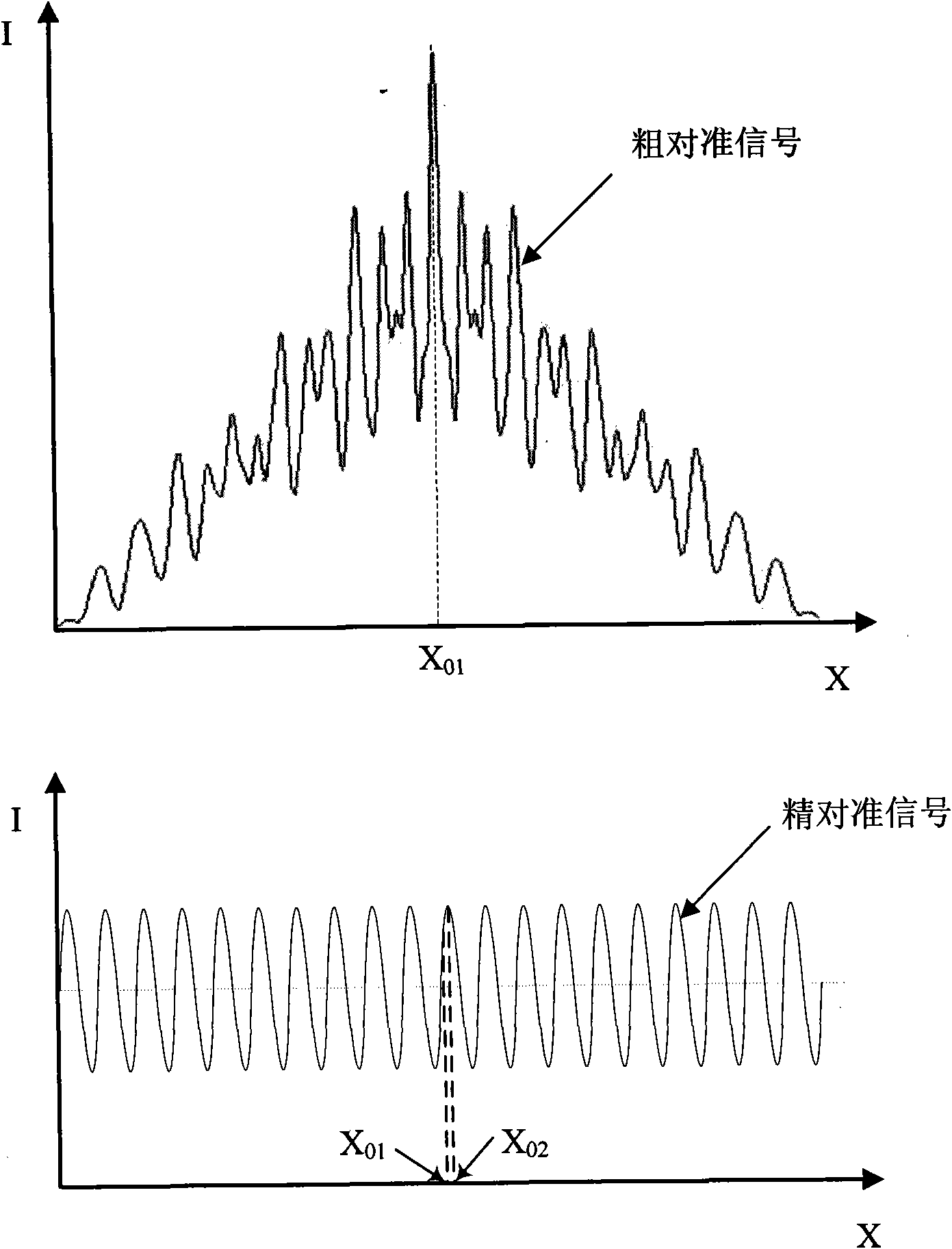
[0028] attached figure 2 The forms of the coarse and ...


PUM


Abstract

The invention discloses an alignment signal processing method based on amplitude and phase probed separately. The method breaks a rough alignment signal from an alignment signal into sections and summarizes the same as well estimates peak value position; determines a rough alignment position of marker by rough alignment signal model fitting; simplifies and summarizes the accurate alignment signal from the alignment signal and determines peak value point of the accurate alignment signal by accurate alignment signal model fitting; and synthesizes the rough alignment position and the accurate alignment signal peak value point to determine a final alignment position. The alignment signal processing method provided by the invention can effectively improve alignment signal processing efficiency to acquire correct alignment position.

Description

technical field [0001] The invention relates to an alignment signal processing method in semiconductor integrated circuit lithography technology, in particular to an alignment signal processing method using separate detection of amplitude and phase. Background technique [0002] The photolithography apparatus in the prior art is mainly used in the manufacture of integrated circuits (ICs) or other micro devices. Through a photolithography device, multi-layer masks with different mask patterns are sequentially imaged under precise alignment on a photoresist-coated silicon wafer, such as a semiconductor silicon wafer or an LCD panel. Lithography devices are generally divided into two categories, one is stepping lithography devices, the mask pattern is exposed and imaged on one exposure area of ​​the silicon wafer, and then the silicon wafer moves relative to the mask to move the next exposure area to the mask. Underneath the mask pattern and the projection objective lens, the ...

Claims


Application Information

Patent Timeline
IPC IPC(8): G03F9/00G03F7/20
Inventor 李运锋王海江赵新陈延太韦学志
Owner SHANGHAI MICRO ELECTRONICS EQUIP (GRP) CO LTD
Why Eureka
Try Eureka