Method for manufacturing integrated circuit

A manufacturing method and technology of integrated circuits, which are applied in the direction of circuits, electrical components, electrical solid devices, etc.

Active Publication Date: 2012-07-18
REALTEK SEMICON CORP
View PDF4 Cites 0 Cited by
  • Summary
  • Abstract
  • Description
  • Claims
  • Application Information

AI Technical Summary

Problems solved by technology

Although this method can simplify the ordering of photomasks and packaging, the communication between hardware units is still limited by the pins of each chip in actual application, and the cost of packaging is not low.

Method used


Image

  • Method for manufacturing integrated circuit
  • Method for manufacturing integrated circuit
  • Method for manufacturing integrated circuit

Examples


Embodiment Construction

[0032] The aforementioned and other technical contents, features and functions of the present invention will be clearly presented in the following detailed description of two preferred embodiments shown with reference to the accompanying drawings.

[0033] Before the present invention is described in detail, it should be noted that in the following description, similar elements are denoted by the same reference numerals.

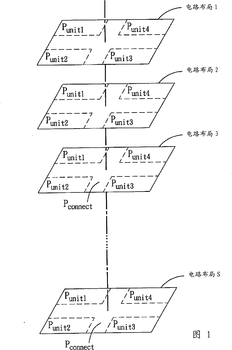
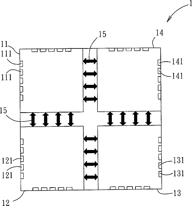
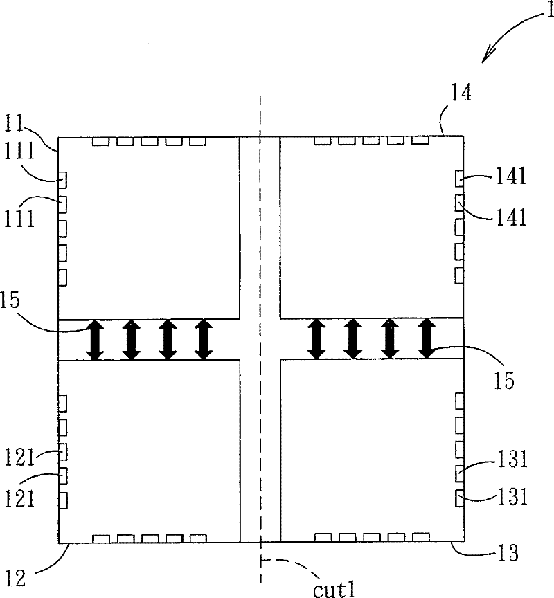
[0034] The preferred embodiment of the integrated circuit manufacturing method of the present invention is suitable for producing a variety of chips including different numbers of hardware units, and each hardware unit can operate independently or combined, for example: each hardware unit can be used as a receiver of a wireless communication system. The main principle is to integrate and route multiple hardware units with similar functions in the S-layer circuit layout (layout), and then after photomask fabrication and chip processing, it is cut and packaged ...


PUM


Abstract

The invention discloses a method for manufacturing an integrated circuit, comprising the following steps: circuit distribution wires of a same hardware unit are distributed at a relative same position of each layer in the S-layer circuit distribution of the integrated distribution wires of a plurality of hardware units; the relative same position of each layer forms an integrated circuit, and a Clayer of S layers is at least connected with the integrated circuits of different hardware units of a same layer through communicating distribution wires; and the communicating distribution wires aregathered at the other relative same position of the C layer of the S layers, wherein the C is a positive integer less than the S, the other relative same position at least includes a width more than that of a cutting passage, and whether the cutting passage is cut can determine the number of generated tube cores and the number of the hardware units included by each tube core.

Description

technical field [0001] The present invention relates to an integrated circuit design and layout technology, in particular to an integrated circuit manufacturing method with photomask reusability. Background technique [0002] In many system applications, multiple hardware units with similar functions are often used to enhance work performance. For example, the communication system improves the receiving capacity by increasing the number of receivers; the computer system uses multiple processors to speed up the calculation speed and increase the loadable calculation capacity. Among them, the number of hardware units required by each system varies with the application level and purpose. [0003] Three methods are known to provide different numbers of hardware units: [0004] The first method is to use a single set of photomasks to fabricate dies including hardware units, and then package multiple dies into chips including a desired number of hardware units according to actua...

Claims


Application Information

Patent Timeline
Patent Type & Authority Patents(China)
IPC IPC(8): H01L21/82H01L27/02H01L23/522G06F17/50
Inventor 杨立平陈碧成康汉彰颜仁鸿
Owner REALTEK SEMICON CORP
Why Eureka
Try Eureka