
Method for cutting silicon chips

A silicon wafer cutting and cutting line technology, which is applied to fine working devices, stone processing equipment, manufacturing tools, etc., can solve the problems of cumulative deviation of cutting lines, waste of cutting lines, and uneven thickness of silicon wafers, so as to reduce the difference in thickness, Effect of improving utilization rate and improving quality

Inactive Publication Date: 2010-01-20
NINGBO SUNEARTH SOLAR POWER
View PDF0 Cites 46 Cited by
  • Summary
  • Abstract
  • Description
  • Claims
  • Application Information

AI Technical Summary

Problems solved by technology

Compared with other traditional cutting technologies, the above-mentioned silicon wafer cutting technology has the advantages of high efficiency, high productivity, and high precision. During the cutting process, the rod is always directional, and it takes about 8 hours to complete the cutting, which causes a large cumulative deviation of the cutting line, which will lead to uneven thickness of the silicon wafer obtained by cutting, or silicon wafers. The quality of the two surfaces of the wafer is not ideal, which ultimately affects the yield of the silicon wafer. On the other hand, the cutting line of this cutting method is always directional during the cutting process of the silicon rod. line, so that the number of wafer cuts per unit length of the cutting line is low

Method used


Image

  • Method for cutting silicon chips

Examples


Embodiment 1

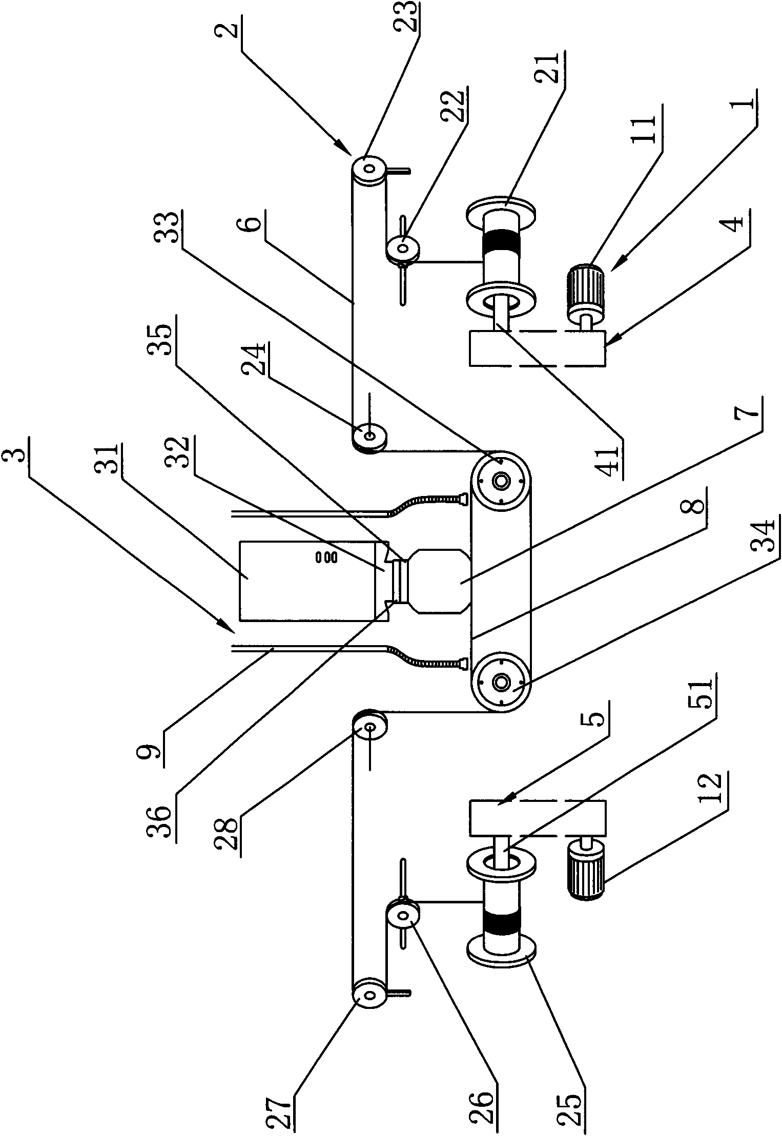
[0014] Embodiment one: the silicon wafer cutting method of the present invention can be used on the existing silicon wafer cutting machine, and existing silicon wafer cutting machine is as figure 1As shown, it includes a housing (not shown in the figure), and a driving device 1, a cable arrangement 2, a cutting chamber 3 and a control system (not shown in the figure) are arranged in the housing. The top of the cutting chamber 3 is provided with a working platform 31, the working platform 31 is provided with a workpiece fixture 32, and the workpiece fixture is movably connected with a splint 36 for clamping the silicon rod 7, and the bottom of the cutting chamber 3 is provided with a first guide wheel 33 and The second guide wheel 34, the first guide wheel 33 is radially provided with a plurality of first wire grooves (not shown in the figure), and the second guide wheel 34 is radially provided with a plurality of wire grooves corresponding to the first wire grooves. The second...

Embodiment 2

[0022] Embodiment two: this implementation is basically the same as embodiment one, and the only difference is that in the present embodiment, the descending speed is set to 25mm / min, the advancing speed is set to 9.5m / s, and the pay-off spool driving motor 11 The line length of driving pay-off spool 21 forward pay-off is set as 250m, and the line length of take-up spool drive motor 12 driving take-up spool 25 reverse pay-off is set as 60m, so when pay-off spool drive motor 11 and take-up spool After the drive motor 12 rotates in the forward direction for about 26.3s, the drive motor 11 of the pay-off spool and the drive motor 12 of the take-up spool need to rotate in the reverse direction, and the time of reverse rotation is about 6.3s. After the bobbin drive motor 12 reversely rotates for 6.3s, the pay-off bobbin drive motor 11 and the take-up bobbin drive motor 12 rotate forwardly again.

Embodiment 3

[0023] Embodiment 3: This embodiment is basically the same as Embodiment 1 and Embodiment 2. The only difference is that in this embodiment, the descending speed is set to 28mm / min, and the traveling speed is set to 11.5m / s. Line spool drive motor 11 drives the line length of pay-off spool 21 forward pay-off to be 265m, and the line length of take-up spool drive motor 12 to drive take-up spool 25 reverse pay-off is set to 60m, so when pay-off spool drive motor After 11 and take-up spool drive motor 12 rotate forward for about 23s, pay-off spool drive motor 11 and take-up spool drive motor 12 need to rotate in reverse, and the time for reverse rotation is about 5.2s. 11 and take-up spool drive motor 12 reversely rotated 5.2s after the pay-off spool drive motor 11 and take-up spool drive motor 12 forwardly rotated again.


PUM

PropertyMeasurementUnit
Line lengthaaaaaaaaaa

Abstract

The invention discloses a method for cutting silicon chips, which comprises the following steps: controlling a pay-off spool driving motor, a take-up spool driving motor, a first guide wheel driving motor and a second guide wheel driving motor to rotate synchronously and inversely by a control system after the pay-off spool driving motor drives a pay-off spool to positively pay off wires for 250m-270m; and controlling the four motors to rotate positively again by the control system after the take-up spool driving motor drives a take-up spool to reversely pay off wires for 60m-70m. A silicon rod is cut back and forth in this way repeatedly like a saw blade dragging type, and because a cutting line moves forward for a certain distance and then moves backward for a certain distance, the utilization ratio of the cutting line is efficiently enhanced without breaking the cutting line. Because the silicon rod is cut back and forth, the thickness up and down each silicon chip is uneven when cutting the silicon rod positively, but the direction of each silicon chip can be effectively corrected in reverse cutting, and thus the thickness difference up and down each silicon chip is greatly reduced so as to enhance the quality of the silicon chips.

Description

technical field [0001] The invention relates to a silicon wafer, in particular to a silicon wafer cutting method. Background technique [0002] With the shortage of energy, more and more people pay attention to photovoltaic power generation, and the market demand for silicon wafers of solar cells is also increasing. Silicon wafers for solar cells are made by cutting square monocrystalline silicon rods into thin slices. However, due to the high price of silicon crystal materials, especially in China, silicon crystal materials are extremely scarce. competitiveness is crucial. [0003] In order to reduce the cost of silicon wafers for solar cells, it is necessary to cut more silicon wafers from a square monocrystalline silicon rod, that is, to make each silicon wafer as thin as possible. Requirements, but also makes the traditional blade cutting method eliminated. Silicon wafer multi-wire cutting technology is a relatively advanced silicon wafer processing technology in the ...

Claims


Application Information

Patent Timeline
IPC IPC(8): B28D5/04
Inventor 徐洪峰贺林丰王作为庄敏
Owner NINGBO SUNEARTH SOLAR POWER
Features
  • Generate Ideas
  • Intellectual Property
  • Life Sciences
  • Materials
  • Tech Scout
  • Unparalleled Data Quality
  • Higher Quality Content
  • 60% Fewer Hallucinations
Learn More