
Metal bump structure and application thereof to packaging structure

A technology of metal bumps and packaging structures, which is applied in the direction of electrical components, electrical solid devices, circuits, etc., can solve the problems of complex manufacturing process, high cost, poor lamination of conductive particles of anisotropic conductive film, etc., and achieve improved capture rate, The effect of reducing churn

Inactive Publication Date: 2010-01-27
HANNSTAR DISPLAY CORPORATION
View PDF0 Cites 7 Cited by
  • Summary
  • Abstract
  • Description
  • Claims
  • Application Information

AI Technical Summary

Problems solved by technology

However, the manufacturing process of this solution is relatively complicated, which not only increases the cost, but also still has the problem of short circuit.
[0006] In addition, some driver IC manufacturers use the concave part of the surface of the metal bump to capture the conductive particles of the anisotropic conductive film. Poor lamination of conductive particles of anisotropic conductive film

Method used


Image

  • Metal bump structure and application thereof to packaging structure
  • Metal bump structure and application thereof to packaging structure
  • Metal bump structure and application thereof to packaging structure

Examples


Embodiment Construction

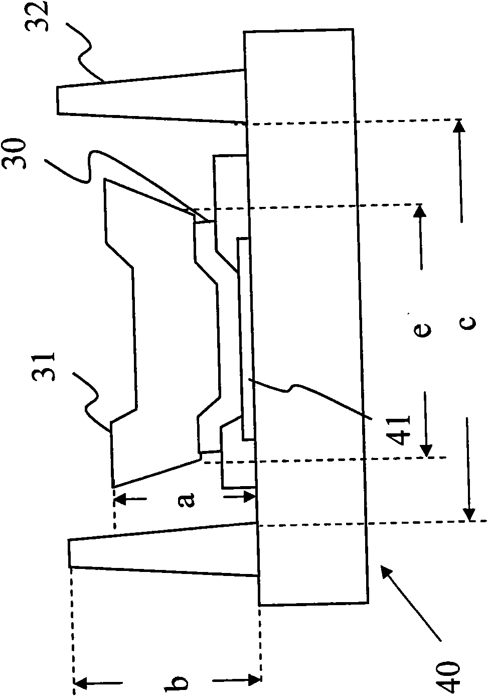
[0046] Please refer to Figure 3A and Figure 3B , are respectively a cross-sectional view and a top view of the metal bump structure provided by the embodiment of the present invention. The metal bump structure mainly includes an under bump metallurgy (UBM) 30 , a metal bump 31 and a barrier layer (dam structure) 32 , wherein the UBM layer 30 is disposed on the connection pad 41 of the semiconductor device 40 and the metal bump 31, and the barrier layer 32 is made of polymer material on the semiconductor element 40, and the barrier layer 32 completely surrounds the metal bump 31, wherein the height b of the barrier layer 32 exceeds The height a of the metal bump 31, such as Figure 3A b>a shown, and the barrier layer 32 is not in contact with the metal bump 31, that is, there is a gap between the barrier layer 32 and the metal bump 31, as Figure 3A c > e shown.

[0047] Please refer to Figure 4A to Figure 4F , the entire process of fabricating the metal bump structure ...


PUM

PropertyMeasurementUnit
heightaaaaaaaaaa
thicknessaaaaaaaaaa

Abstract

The invention relates to a metal bump structure and application thereof to a packaging structure. A dam structure higher than a metal bump is arranged around the metal bump, so the dam structure can obstruct and limit the flow of conductive particles in each anisotropic conductive film (ACF) in a flip chip jointing process. In addition, as the dam structure is made from a high molecular material and the thermal resistance of the dam structure is higher than that of the metal bump, the metal bump structure generates flow differences between the anisotropic conductive films to reduce the loss of the conductive particles and improve the capture rate of the conductive particles.

Description

【Technical field】 [0001] The invention relates to a chip-on-glass (COG) assembly technology, in particular to a metal bump structure and its application to a package structure. 【Background technique】 [0002] Chip on Glass (COG) is a module assembly technology for high pin count and fine pitch Flat Panel Display. The technical feature of this module assembly is that there are minimum joints between the driver IC signal source and the panel glass substrate, and it does not require the use of flexible substrates. Therefore, it can overcome the tendency of the tape and reel package (TCP) to be easily caused by bending. The phenomenon of foot breakage, thereby improving the reliability of the product. [0003] Currently, the COG technology uses an anisotropic conductive film (Anisotropic Conductive Film; ACF) as a medium for conductive bonding. Please refer to figure 1 , the anisotropic conductive film 10 is a polymer material, which is formed by uniformly mixing the conducti...

Claims


Application Information

Patent Timeline
Patent Type & Authority Applications(China)
IPC IPC(8): H01L23/485H01L23/488
CPCH01L24/11H01L2224/11H01L2924/00012
Inventor 汤宝云
Owner HANNSTAR DISPLAY CORPORATION
Learn More