

Method for manufacturing image display
A technology of an image display device and a manufacturing method, which is applied in the directions of identification devices, nonlinear optics, optics, etc., can solve the problems of uncured, insufficient light reaching, etc., and achieve the effect of preventing orientation disorder
- Summary
- Abstract
- Description
- Claims
- Application Information
AI Technical Summary
Problems solved by technology
Method used
Image

Examples
Embodiment
[0094] Hereinafter, the present invention will be specifically described with reference to experimental examples, but the present invention is not limited to the following examples.
[0095] The following resin compositions a to h were prepared.
[0096] Resin composition a
[0097] Mix 50 parts by weight of urethane acrylate (trade name UV-3000B, manufactured by Nippon Synthetic Chemical Industry Co., Ltd.), 30 parts by weight of isobornyl acrylate (trade name IBXA, manufactured by Osaka Organic Chemical Industry Co., Ltd.), Organic peroxide (trade name PERBUYL O, manufactured by NOF Corporation) 5 parts by weight, photopolymerization initiator (trade name IRGACURE 184, manufactured by Ciba Specialty Chemicals Co., Ltd.) 3 parts by weight, and photopolymerization initiator ( Resin composition a was prepared in 1 part by weight of SpeedCure TPO (trade name, manufactured by Nihon Siber Hegner K.K.).
[0098] Resin composition b
[0099] Without adding organic peroxides, uret...
experiment example 1-1
[0112] Experimental Example 1-1 [Curing Rate of Resin Composition]
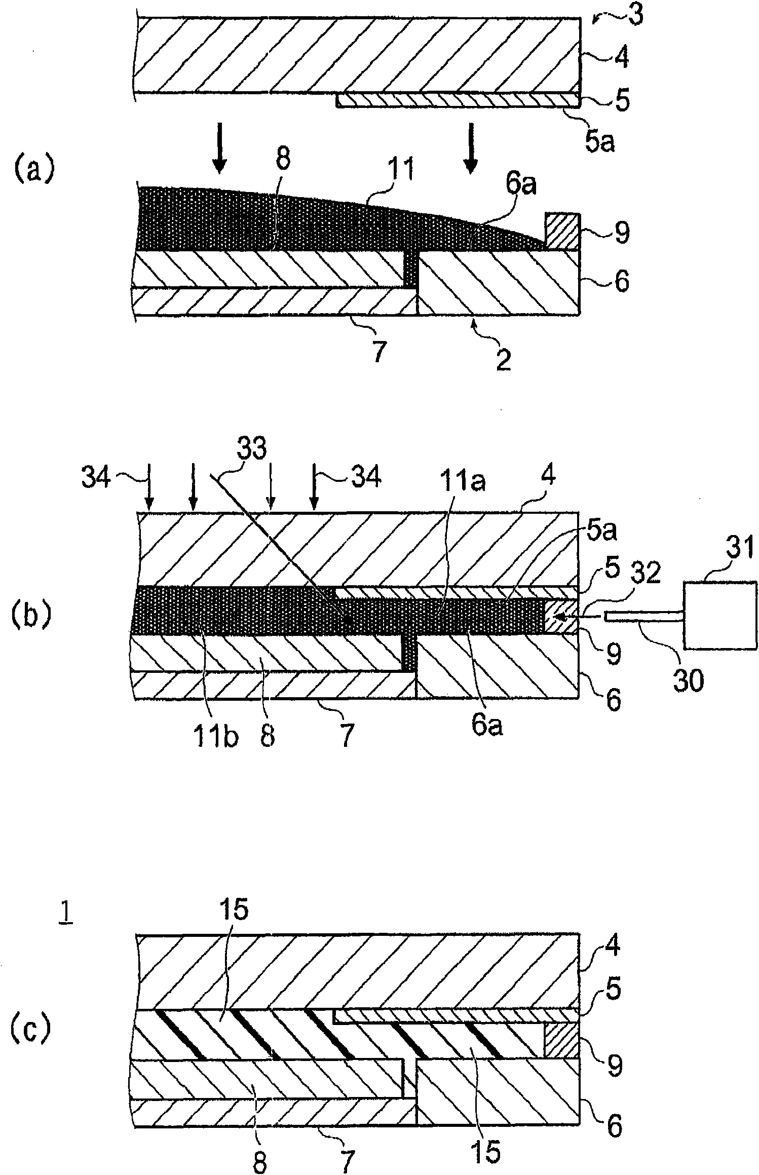
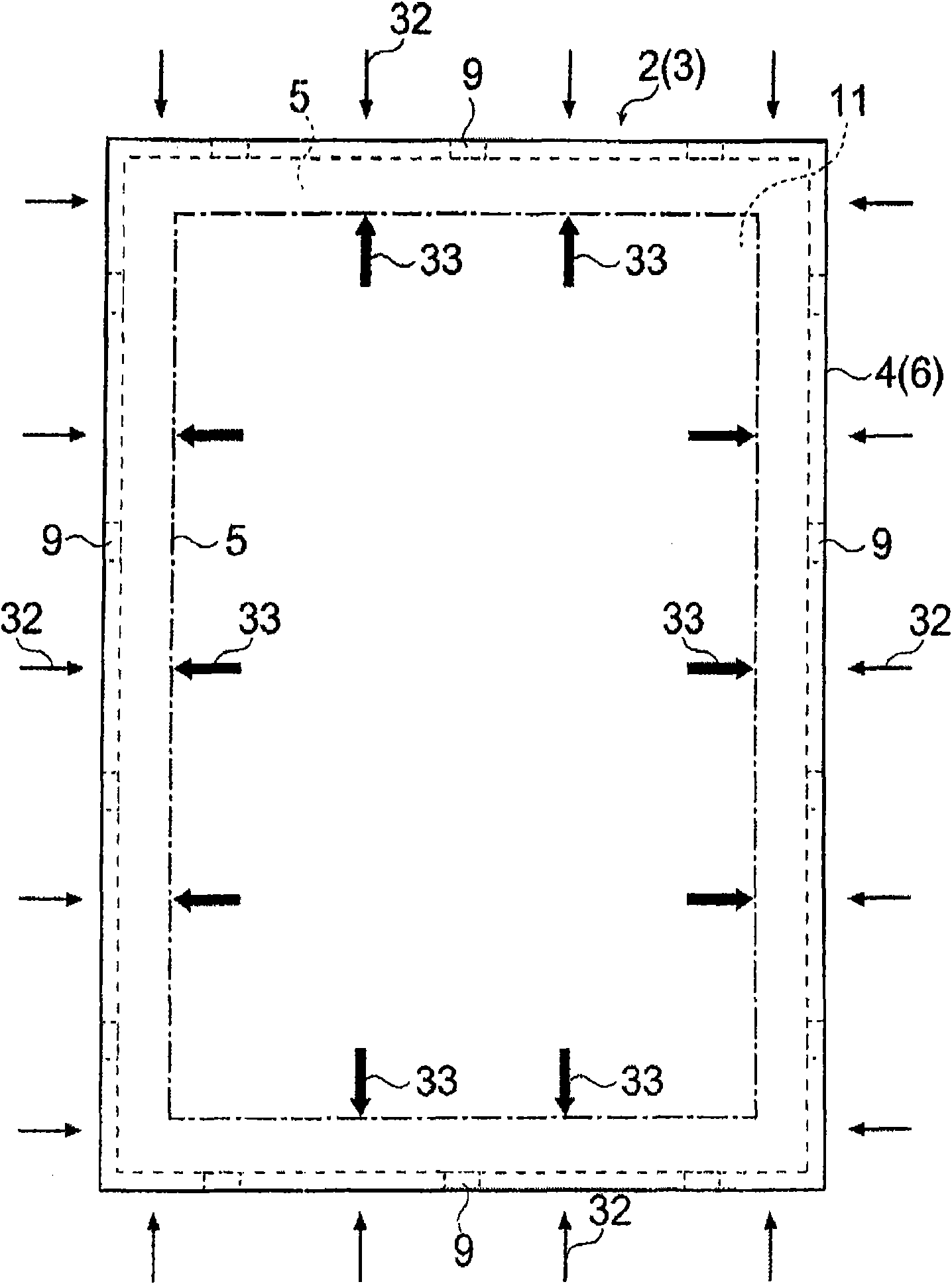
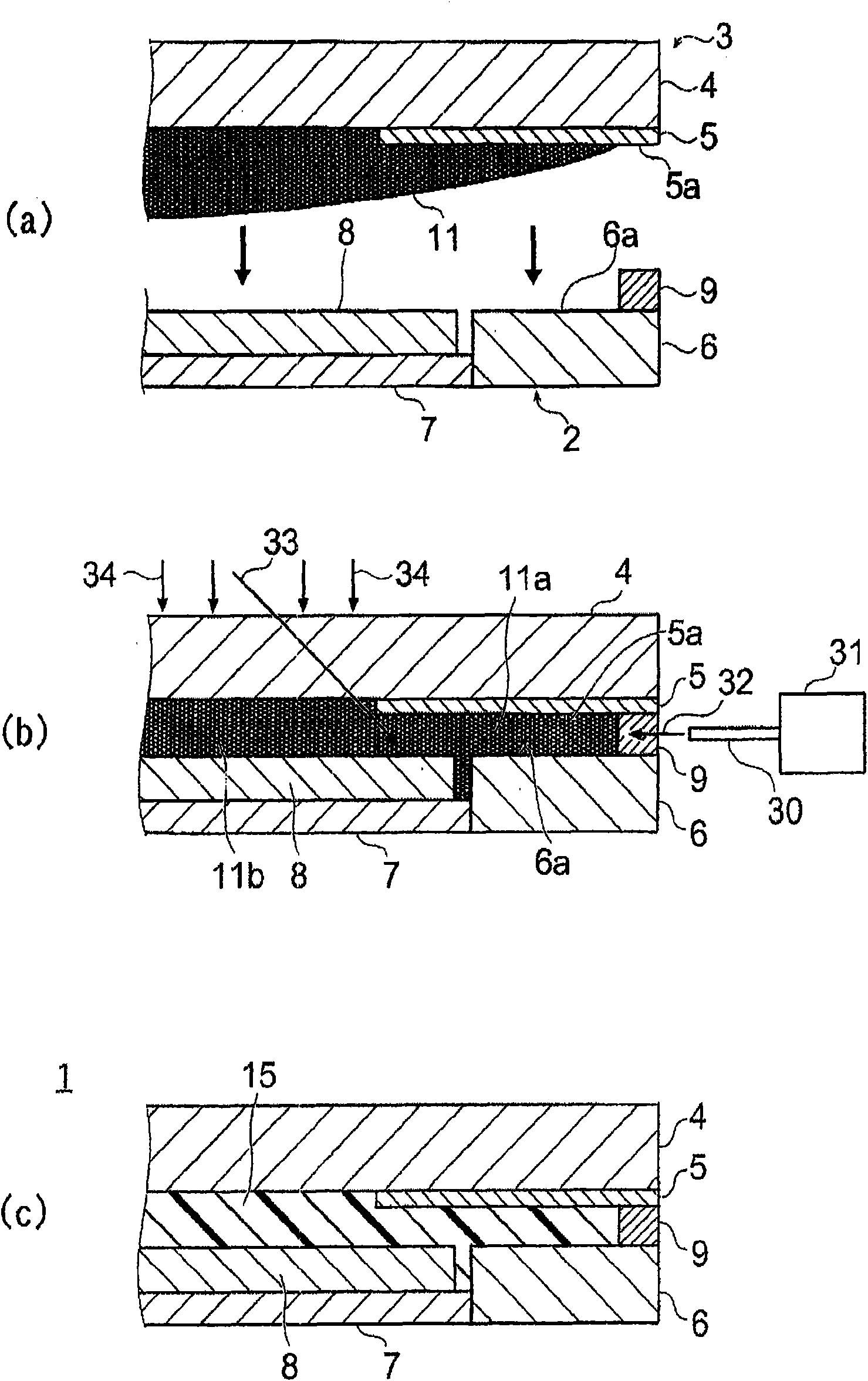
[0113] Make resin composition a and resin composition b respectively to such as figure 1 0.2 g of the spacer inside the liquid crystal display substrate shown in (a) was dropped, and an acrylic plate having a light-shielding portion with a width of 2.0 mm as a protective part was placed on the spacer, and then, under the following curing conditions A to In D, the resin compositions were respectively photocured, and as shown in Table 1, a liquid crystal display device was fabricated.
[0114] Then, the obtained acrylic plate of the liquid crystal display device was peeled off, and the curing rates of the cured products of the respective resin compositions a and b were measured as described below. Record the results in Table 1.
[0115] Curing condition A:
[0116] Using a UV lamp (manufactured by USHIO Electric Co., Ltd.), ultraviolet rays with a cumulative light intensity of 5000 mJ were irradiated from a...
experiment example 1-2
[0128] Except for using an acrylic plate having a light-shielding portion with a width of 5.0 mm as the protective portion, a liquid crystal display device was fabricated using the resin compositions a and b in the same manner as in Experimental Example 1-1, and the curing conditions were changed, and the obtained liquid crystal display device was measured. The curing rate of the cured resin in. Record the results in Table 2.
[0129] [Table 1]
[0130] Experimental example 1-1 (shading part 2mm)
[0131]
[0132] Curing condition A: UV rays are irradiated from only one side of the acrylic sheet
[0133] Curing condition B: UV rays are irradiated from the side of the acrylic sheet and heated with a heater
[0134] Curing condition C: UV rays are irradiated from one side of the acrylic sheet and UV rays are irradiated from the side side
[0135] Curing condition D: UV radiation is irradiated from an acrylic plate, heated by a heating table, and UV radiation is irradiated...
PUM
| Property | Measurement | Unit |
|---|---|---|
| Storage elasticity | aaaaa | aaaaa |
| Storage elasticity | aaaaa | aaaaa |
| Thickness | aaaaa | aaaaa |
Abstract
Description
Claims
Application Information