Clock data recovery circuit, method and test device utilizing them

A clock data recovery and testing device technology, applied in electronic circuit testing, measuring devices, synchronization devices, etc., can solve problems such as inability to obtain phase information correctly, inability to estimate the amount of serial data jitter, etc.

Active Publication Date: 2010-02-24
ADVANTEST CORP
View PDF2 Cites 19 Cited by
  • Summary
  • Abstract
  • Description
  • Claims
  • Application Information

AI Technical Summary

Problems solved by technology

However, the following problems were recognized: when using a CDR circuit using a PLL circuit, since the frequency of the strobe signal is adjusted, its phase information cannot be acquired correctly, and the amount of jitter possessed by the serial data cannot be estimated

Method used


Image

  • Clock data recovery circuit, method and test device utilizing them
  • Clock data recovery circuit, method and test device utilizing them
  • Clock data recovery circuit, method and test device utilizing them

Examples


Embodiment Construction

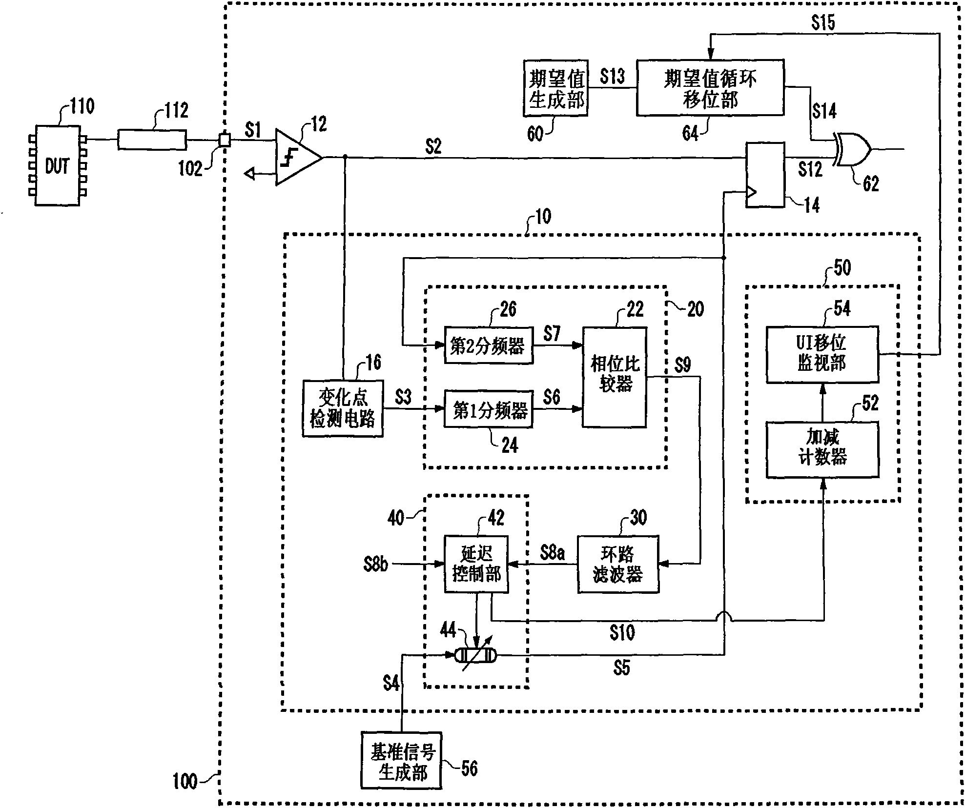
[0032] Hereinafter, the present invention will be described based on preferred embodiments with reference to the drawings. The same or equivalent structural elements, components, and processes shown in the drawings are denoted by the same symbols, and overlapping descriptions are appropriately omitted. In addition, the embodiment is not an illustration to limit the invention, and all the features or combinations thereof described in the embodiment are not necessarily the essential content of the invention.

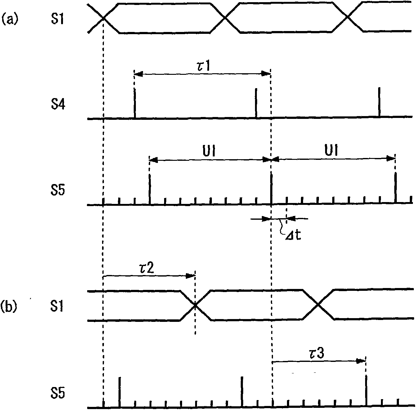
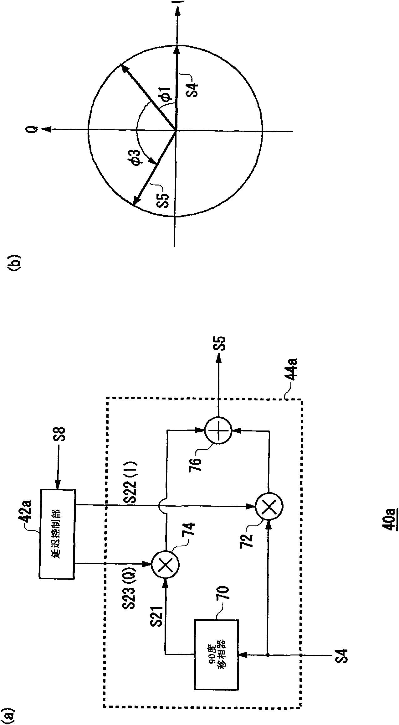
[0033] figure 1 It is a block diagram showing the configuration of a test device 100 using the clock data recovery circuit 10 according to the embodiment of the present invention. The test device 100 receives the serial data S1 output from the DUT 110 connected via the transmission line 112 , and checks the DUT 110 by comparing with the expected value data S13 .

[0034] First, an outline of the overall configuration of the test device 100 will be described. The test de...


PUM


Abstract

A change point detection circuit (16) extracts a clock signal (S3) from an input data, i.e. a serial data (S1). A variable delay circuit (40) imparts a delay dependent on a delay control signal (S8a)to a reference signal (S4) having a predetermined frequency, and shifts the phase of the reference signal (S4) with reference to an initial delay. An input latch circuit (14) latches internal serial data (S2) using the output signal from the variable delay circuit (40) as a strobe signal (S5). A phase comparator (22) matches the frequencies of the clock signal (S3) and the strobe signal (S5) and generates phase difference data (S9) dependent on the phase difference of two signals. A loop filter (30) integrates the phase difference data (S9) generated by the comparator (22) and outputs the delay control signal (S8a). A phase shift amount acquisition section (50) acquires the amount of phase shift with reference to the initial delay imparted to the reference signal by the variable delay circuit (40) based on the delay control signal (S8a).

Description

technical field [0001] The invention relates to a clock data recovery technique for regenerating input bit stream data by using a strobe signal. Background technique [0002] In order to use few data transmission lines to send and receive data between semiconductor circuits, serial data transmission is adopted. Serial data transmission can adopt CDR (Clock and Data Recovery: clock data recovery) mode or source synchronous (Source Synchronous) mode. In the CDR method, 8B10B encoding or 4B5B encoding is used so that serial data does not continuously take the same value over a predetermined period, and a clock signal for synchronization is embedded in the serial data. [0003] When testing a semiconductor circuit that outputs serial data as a device under test (DUT), a CDR circuit is provided in an input stage of a semiconductor test device (also simply referred to as a test device). The CDR circuit extracts the reference clock signal from the serial data, and generates a str...

Claims


Application Information

Patent Timeline
Patent Type & Authority Applications(China)
IPC IPC(8): H03K5/00G01R29/02G01R31/28H04L7/033H04L25/02
CPCH03L7/0812H04L7/033G01R31/31937H04L7/0037G01R31/31727H03L7/081G01R29/02G01R31/28H04L25/02
Inventor 渡边大辅冈安俊幸
Owner ADVANTEST CORP
Why Eureka
Try Eureka