Circuit board framing device and drilling and milling device with image framing

An image positioning and circuit board technology, applied in the direction of electrical components, electrical components, manufacturing tools, etc., can solve the problems of pin diameter, hole diameter and position deviation of drilling holes, precision deviation, single function, etc., to achieve a simple and fast processing process. , The effect of improved machining accuracy and high alignment accuracy

Inactive Publication Date: 2010-03-03
邓智军
View PDF0 Cites 13 Cited by
  • Summary
  • Abstract
  • Description
  • Claims
  • Application Information

AI Technical Summary

Problems solved by technology

There is a precision deviation between the patch layer and the drill layer of the printed circuit board, and there are deviations in the diameter of the drill nozzle, the diameter of the pin, the diameter of the hole after drilling, and the hole position, which is not good for the accuracy of the subsequent transplantation of the printed circuit board.
Moreover, when cutting multi-connected printed circuit boards, it is necessary to control the depth for precise cutting. Only one circuit board can be processed at a time. Using a single observation lens for image positioning can only ensure the accuracy of single-axis CNC cutting and forming, and the cost of use is high. , slow
[0004] When transplanting and installing precision positioning of multi-connected printed circuit boards, since the post-process SMT mounting components are all based on the silk screen pad layer, the pin positioning can only be positioned based on the drilling point, and the accuracy of the two reference points is inconsistent; at the same time There are deviations in pin diameter, hole diameter, and drilling hole position, resulting in low precision and poor reliability of transplanted finished printed circuit boards
The mold is used to position multi-connected printed circuit boards. The molds mostly use the appearance layer of multi-connected printed circuit boards as the positioning standard, while the printed appearance of multi-connected circuit boards is mostly positioned and cut by multi-piece laminated pins of CNC machine tools or stamping machine tools. Stamping forming, the above two forming methods lead to low precision of multi-connected printed circuit boards, and the circuit boards placed in the mold are often too tight or too loose, resulting in low precision and poor reliability of transplanted finished printed circuit boards
However, the CCD automatic positioning and transplantation device is used to position the multi-connected printed circuit boards. The single machine is expensive, the use cost is high, the penetration rate is low, and the function is single.
[0005] In summary, the existing multi-connected printed circuit board calibration device and drilling and milling device obviously have inconvenience and defects in actual use, so it is necessary to improve them

Method used


Image

  • Circuit board framing device and drilling and milling device with image framing
  • Circuit board framing device and drilling and milling device with image framing
  • Circuit board framing device and drilling and milling device with image framing

Examples


Embodiment Construction

[0039] In order to make the object, technical solution and advantages of the present invention clearer, the present invention will be further described in detail below in conjunction with the accompanying drawings and embodiments. It should be understood that the specific embodiments described here are only used to explain the present invention, not to limit the present invention.

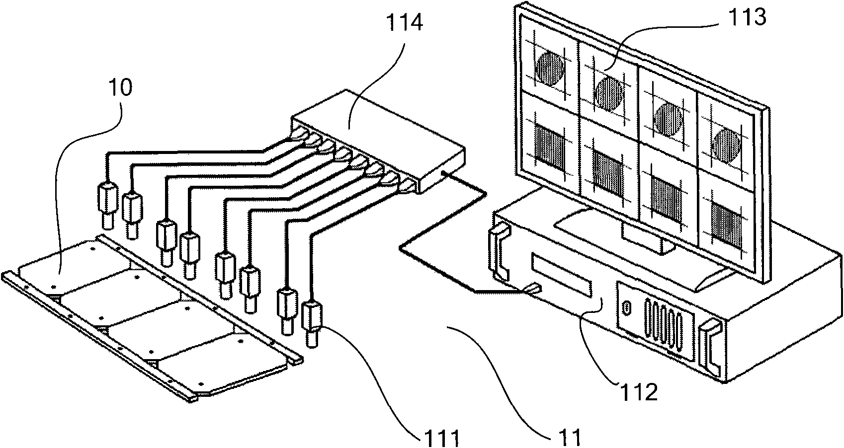
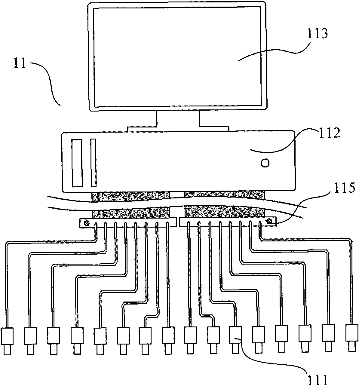
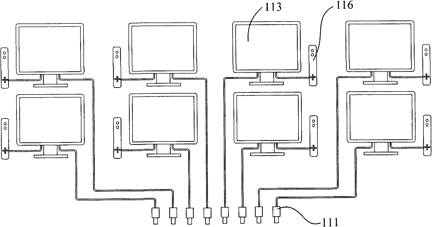
[0040] Such as Figure 1 to Figure 10 As shown, a circuit board alignment device 100 with image positioning in the present invention includes an image positioning device 11 for correcting the position of the multi-circuit board 10, and the image positioning device 11 includes:

[0041] A plurality of observation lenses 111 are respectively aimed at a plurality of marking points on the multi-connected circuit board 10, and are used to capture image data of the multi-connected circuit board 10, and the image data includes optical points in the multi-connected circuit board 10, The observation lens 1...


PUM


Abstract

The invention discloses a circuit board framing device and a drilling and milling device with image framing, comprising a framing device for regulating the position of multiple circuit boards. The framing device comprises a plurality of viewing lens which is arranged for aiming at a plurality of marking points on the multiple circuit boards and retrieving the imaging data of the multiple circuit boards, a processor connected to the viewing lens and arranged for processing the imaging data, a display unit connected to the viewing lens and/or the processor for displaying the imaging data of themultiple circuit boards. The invention respectively observes the marking points on the multiple circuit boards by a plurality of viewing lens and views and compares the imaging data of the multiple circuit boards in the display unit. The microscopic sharp image can be acquired by observing separate marking points with separate viewing lens and the framing precision is high.

Description

technical field [0001] The invention relates to the field of electronic circuit boards, in particular to a circuit board alignment device and a drilling and milling device with image positioning. Background technique [0002] As the assembly requirements of the electronics industry continue to increase, the requirements for the carrier printed circuit board of electronic components also increase accordingly. At present, it has become a basic requirement for many downstream SMT (Surface Mounted Technology, Surface Mount Technology) manufacturers not to allow unit scrapping in finished product shipment units. When CNC equipment is cut and formed, pin positioning and single observation lens image positioning are often used for cutting and forming; when multi-connected printed circuit boards are transplanted for precision positioning and installation, pin positioning, mold positioning and CCD (Charge Coupled Device, charge coupled device) are often used. coupling device) to aut...

Claims


Application Information

Patent Timeline
Patent Type & Authority Applications(China)
IPC IPC(8): H05K13/08H05K13/00B23P23/02
Inventor 邓智军
Owner 邓智军
Why Eureka
Try Eureka