Active array base plate
An active array and substrate technology, applied in optics, instruments, electrical components, etc., can solve problems such as copper wire erosion, copper residual edge angle, poor quality, etc.
- Summary
- Abstract
- Description
- Claims
- Application Information
AI Technical Summary
Problems solved by technology
Method used
Image
Examples
Embodiment Construction
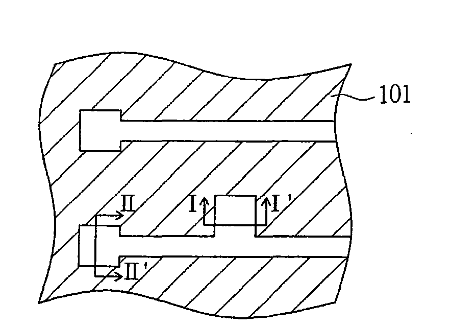
[0065] 1A, 2A, 3A, 4A, 5A, 6A, 7A, 8A, 9A, 10A, and 11A are the top views corresponding to the steps of the manufacturing method of the active array substrate according to an embodiment of the present invention. For the convenience of explanation and understanding, the top views are selectively displayed in perspective.
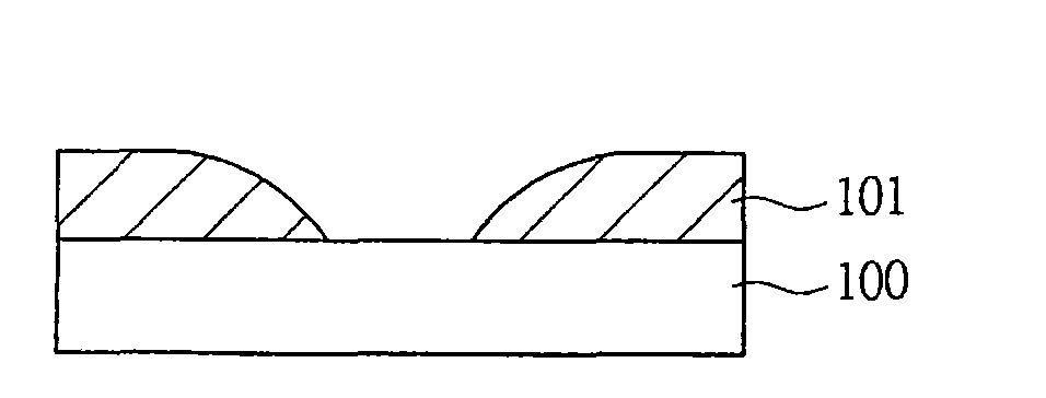
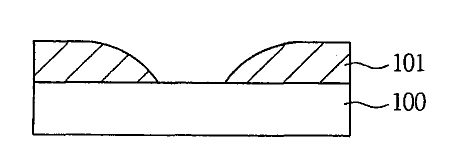
[0066] Please refer to Figure 1A to Figure 1C . Figure 1B and 1C respectively Figure 1A Sectional views along section lines I-I' and II-II'. It should be noted that the position corresponding to the section line I-I' is where the thin film transistors of the active array substrate are manufactured. Such as Figure 1B and 1C As shown in the figure, first, a substrate 100 is provided, and then a patterned photoresist layer 101 is formed on the substrate 100 .
[0067] Please refer to Figure 2A to Figure 2C . Figure 2B and 2C respectively Figure 2A Sectional views along section lines I-I' and II-II'. Using the patterned photoresist layer 101 as ...
PUM
 Abstract
Description
Claims
Application Information


