
Aspheric optical element surface shape detection device

A technology for detecting optical components and surface shape, which is applied in the direction of using optical devices, measuring devices, instruments, etc., can solve the problems of computational hologram processing, assembly and adjustment difficulties, etc., to shorten the detection cycle, reduce the deviation, and reduce the detection cost Effect

Active Publication Date: 2010-03-17
CHINA NORTH IND NO 205 RES INST
View PDF0 Cites 12 Cited by
  • Summary
  • Abstract
  • Description
  • Claims
  • Application Information

AI Technical Summary

Problems solved by technology

[0003] The purpose of the present invention is to overcome the disadvantages of computational hologram processing and assembly difficulties in detecting the surface shape of aspheric optical elements with computational holographic technology, and to provide a method based on two-step phase shift technology, computational holographic technology and digital holographic interference technology. Aspherical optical element surface shape detection device to realize high-precision detection of aspheric optical element surface shape with large asphericity and large surface steepness

Method used


Image

  • Aspheric optical element surface shape detection device
  • Aspheric optical element surface shape detection device
  • Aspheric optical element surface shape detection device

Examples


Embodiment Construction

[0013] The present invention will be further described in detail below in conjunction with the accompanying drawings and preferred embodiments.

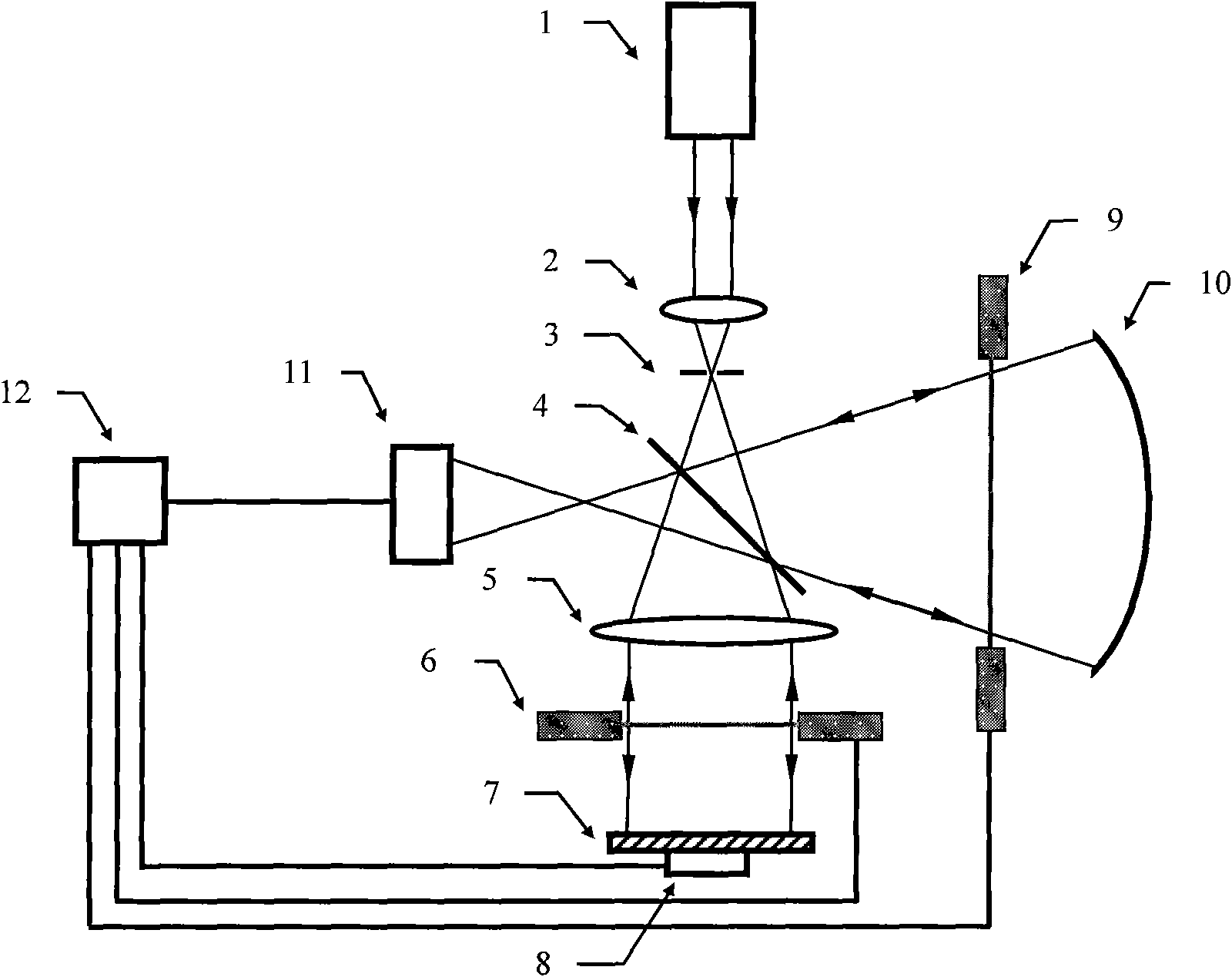
[0014] according to figure 1 As shown, the aspherical optical element surface shape detection device of the present invention includes a helium-neon laser 1, a microscope objective lens 2, a pinhole filter 3, a beam splitter 4, an aplanatic lens 5, a first controllable diaphragm 6, a standard plane Mirror 7, piezoelectric ceramics 8, second controllable aperture 9, CCD detector 11, computer 12. The operating wavelength of the helium-neon laser 1 is 632.8nm, the magnification of the microscope objective lens 2 is 100, the diameter of the pinhole filter 3 is 5 μm, and the beam splitter 4 is a semi-transparent and half-reflective 45° right-angle prism, and the splitting ratio of the splitting surface is is 1:1, the surface shape accuracy of the standard plane mirror 7 is better than λ / 20 and placed on the piezoelectric ceramic 8, the p...


PUM


Abstract

The invention discloses an aspheric optical element surface shape detection device. Based on prior interference method surface shape detection devices, the aspheric optical element surface shape detection device realizes the measurement of the light intensities of detection light waves and reference light waves by additionally arranging two controllable optical stops and can acquire phase shift interference fringes by additionally arranging piezoelectric ceramics. An aspheric surface shape measurement software package can conveniently acquire a phase offset between the surface shape and an ideal surface shape of an aspheric optical element to be detected by computing the phase offset between the surface shape to be detected and a standard surface shape of the aspheric optical element to bedetected and the phase offset between the ideal surface shape and the standard surface shape of the aspheric optical element to be detected. Therefore, the aspheric optical element surface shape detection device can effectively solve the surface shape detection problem of aspheric optical elements with large offset without a practical processing computed hologram, thereby reducing detection cost,shortening detection cycle and improving detection accuracy.

Description

technical field [0001] The invention relates to the technical field of optical precision measurement, in particular to an aspheric optical element surface shape detection device capable of detecting large asphericity. Background technique [0002] Until now, the quantitative detection of the surface shape of aspheric optical elements is still a challenge in the field of optical metrology. The main reason is that there is no corresponding standard aspheric surface template for standard detection, resulting in too dense interference fringes in interference detection, which cannot satisfy the sampling theorem. Currently used solutions include sub-aperture splicing and compensation. The sub-aperture splicing method uses precise mechanical movement to detect different sub-areas of the aspheric optical element, and then stitches each detection result into the surface shape detection result of the entire aspheric optical element. The compensation method uses a compensation mirror...

Claims


Application Information

Patent Timeline
IPC IPC(8): G01B11/24
Inventor 范琦杨鸿儒黎高平
Owner CHINA NORTH IND NO 205 RES INST
Learn More