

Keyboard panel
A keyboard and substrate technology, applied in the direction of electrical connection of printed components, printed circuit components, electrical components, etc., can solve the problems of high manufacturing cost and numerous manufacturing processes, and achieve the effect of reducing manufacturing cost, reducing manufacturing process and low cost.
- Summary
- Abstract
- Description
- Claims
- Application Information
AI Technical Summary
Problems solved by technology
Method used
Image

Examples
Embodiment 1
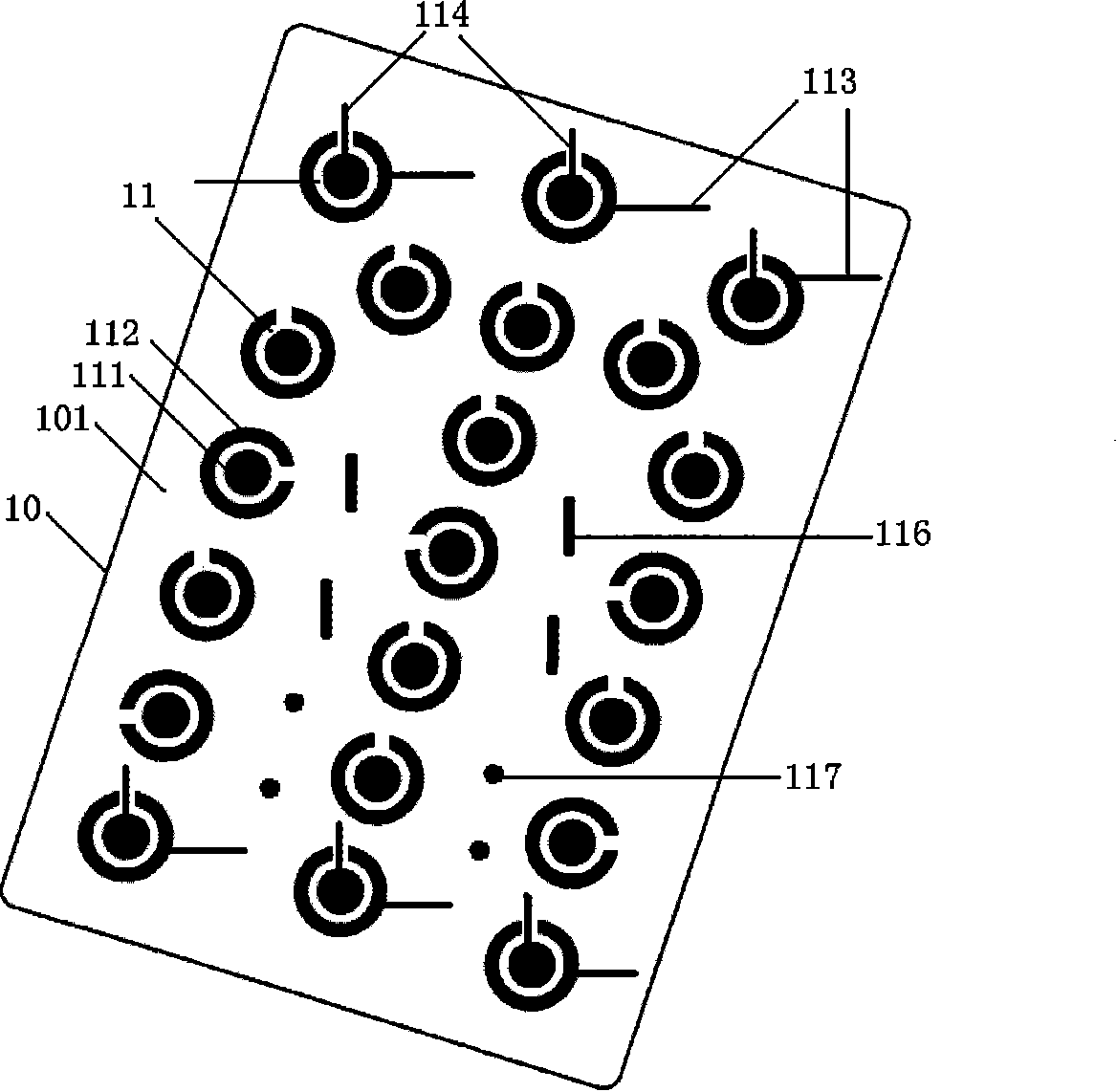
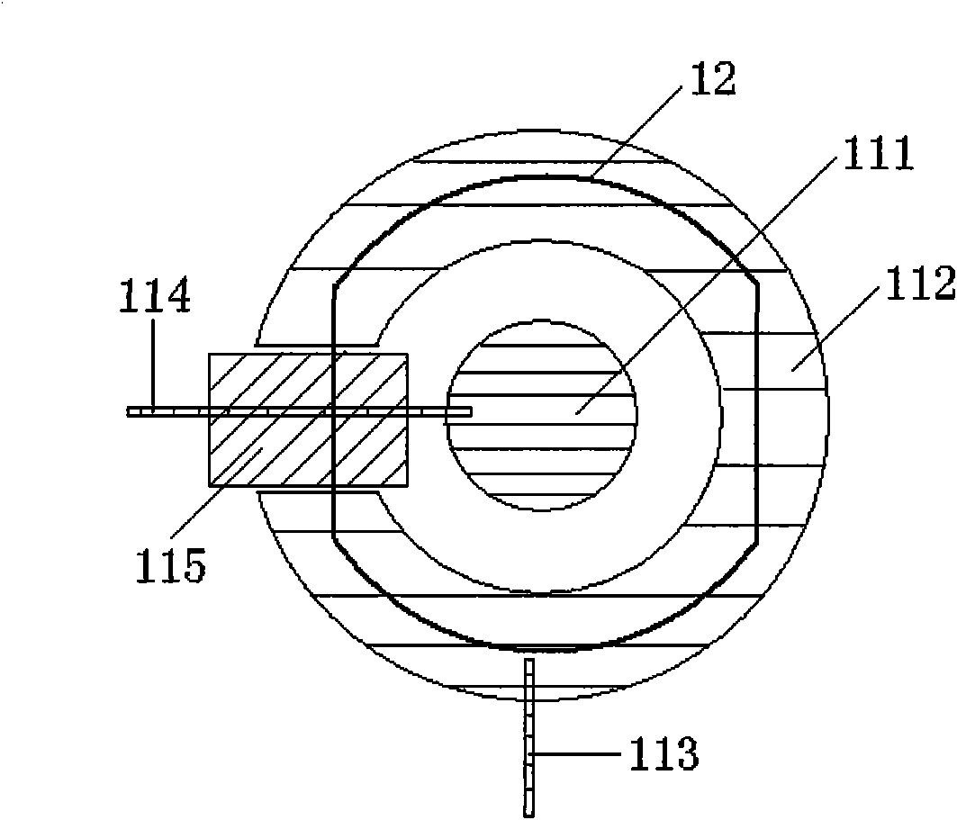
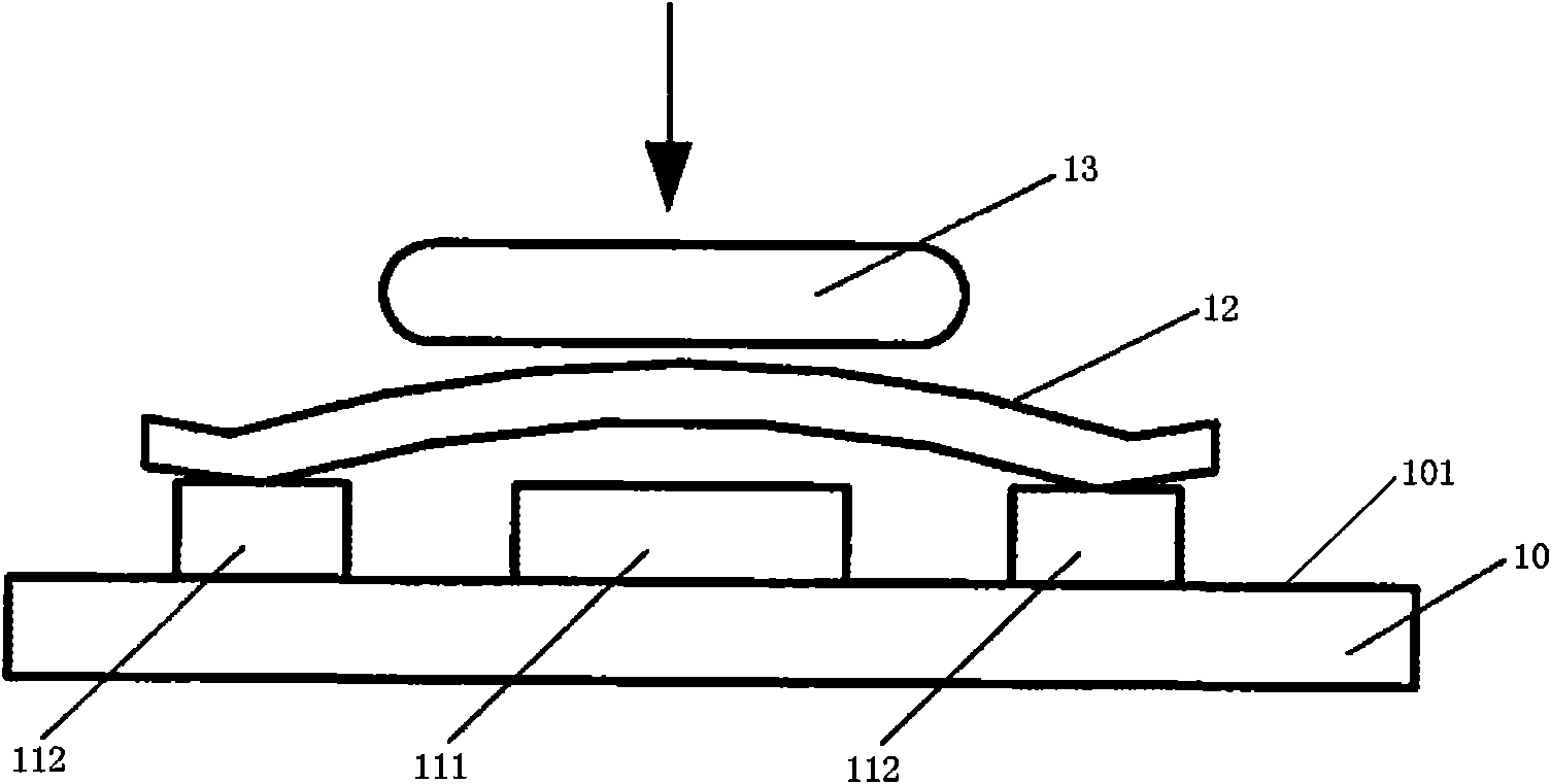
[0020] This embodiment provides a keyboard board, such as figure 1 , figure 2 As shown, the keyboard board includes: a PCB substrate 10, a plurality of key pads 11 arranged on the first surface 101 of the PCB substrate 10 through carbon film printing patterns; the key pads 11 include an inner ring 111 and an outer The ring 112 is on the first surface 101 of the PCB substrate 10 , and the outer ring 112 is connected by a carbon film wiring 113 .
[0021] Wherein, the carbon film has conductivity; the PCB substrate 10 can be made of FR4 (epoxy fiberglass board) material, but not limited thereto.
[0022] In order to complete all the lines on the same layer, the outer ring 112 of the button pad 11 is open to form a non-closed ring. On the first surface 101 of the PCB substrate 10, the inner ring 111 passes through the The opening of the outer ring 112 is connected by a carbon film wiring 114. In this way, the inner ring 111 can also realize the surface wiring. All lines are c...
Embodiment 2
[0039] Different from the first embodiment, the second surface of the PCB substrate can also be printed with a carbon film pattern, and the outer ring of the key pad forms a closed ring.
[0040] Such as Figure 5 , Figure 6 As shown, the outer ring 112 of the button pad 11 forms a closed ring, and a through hole 14 is opened at the position of the inner ring 111 of the button pad 11 on the first surface 101 of the PCB substrate 10. The through hole 14 is plugged with carbon film, and the inner ring 111 of the button pad 11 passes through the through hole 14 , and is connected with the carbon film wiring 15 on the second surface 102 of the PCB substrate 10 .
[0041] Wherein, the implementation of the key graphics, wiring, current adjusting resistors, devices or graphics connected to other single boards, backlight and large-area ground network of the keyboard board is the same as that of Embodiment 1, and will not be repeated here. .
[0042]The keyboard board of the embod...
Embodiment 3
[0044] Same as Embodiment 1, the outer ring opening of the button pad 11 in this embodiment forms a non-closed ring, and all the lines can be completed on the first surface of the PCB substrate; the difference from Embodiment 1 is , the second surface of the PCB substrate can also be printed with carbon film graphics.
[0045] Such as Figure 7 As shown, the first surface 101 of the PCB substrate 10 is provided with a ground network 16 with a carbon film printed pattern, and the second surface 102 of the PCB substrate 10 is fully laid with a ground network 17 with a carbon film printed pattern. The first surface 102 of the PCB 10 is provided with a through hole 18 at the position where the ground network 16 is provided, and the through hole 18 is plugged with a carbon film; thus, the ground network 17 of the second surface 102 of the PCB substrate 10 can pass through the The through hole 18 is connected to the ground network 16 of the first surface 101 of the PCB substrate 10...
PUM
 Abstract
Description
Claims
Application Information