Printed wiring board and method for manufacturing the same

A technology for printed wiring substrates and manufacturing methods, applied in printed circuit manufacturing, printed circuits, printed circuits, etc., can solve the problems of signal frequency band degradation and signal frequency band degradation of printed wiring substrates, achieve characteristic impedance matching, and suppress characteristic impedance loss. The effect of matching and suppressing electromagnetic coupling

Inactive Publication Date: 2010-03-24
NEC CORP
View PDF9 Cites 11 Cited by
  • Summary
  • Abstract
  • Description
  • Claims
  • Application Information

AI Technical Summary

Problems solved by technology

In recent years, the frequency of signals transmitted within devices or between devices has been increasing, and the frequency band of signals in printed wiring boards may be degraded.
In particular, the degradation of the signal band at the via hole in the printed wiring substrate of the multilayer wiring structure is fatal for improving the processing capability

Method used


Image

  • Printed wiring board and method for manufacturing the same
  • Printed wiring board and method for manufacturing the same
  • Printed wiring board and method for manufacturing the same

Examples


Embodiment 1

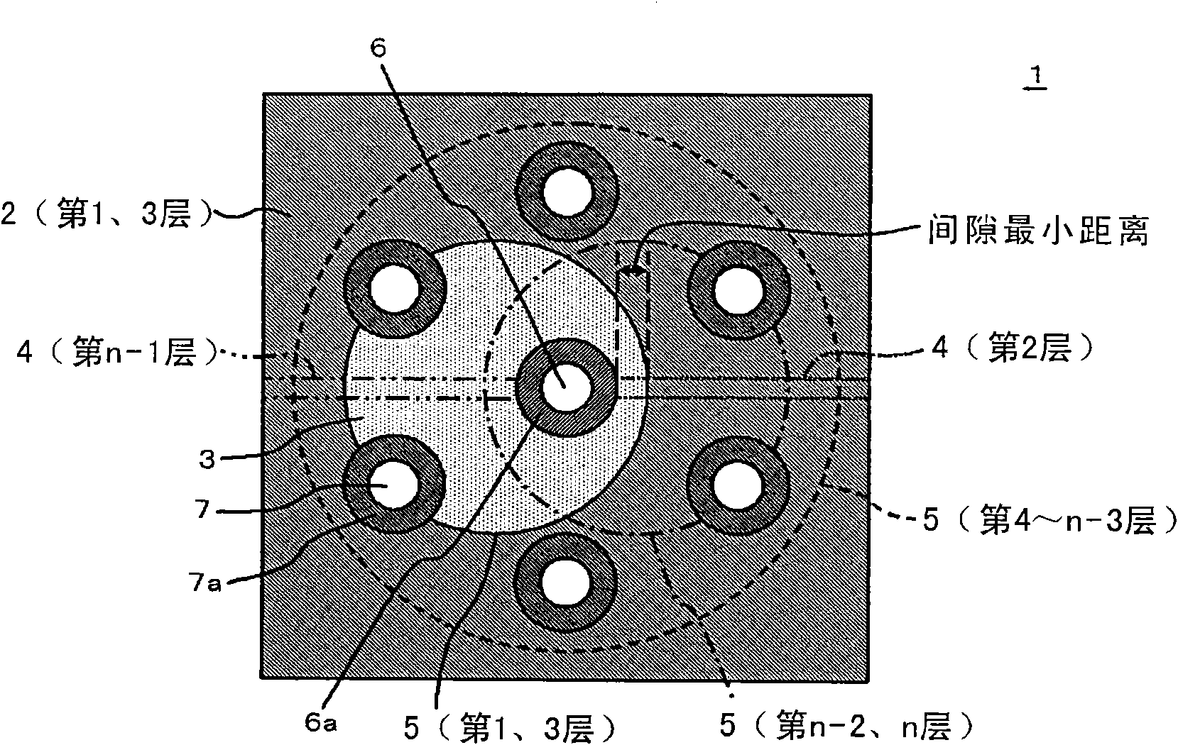
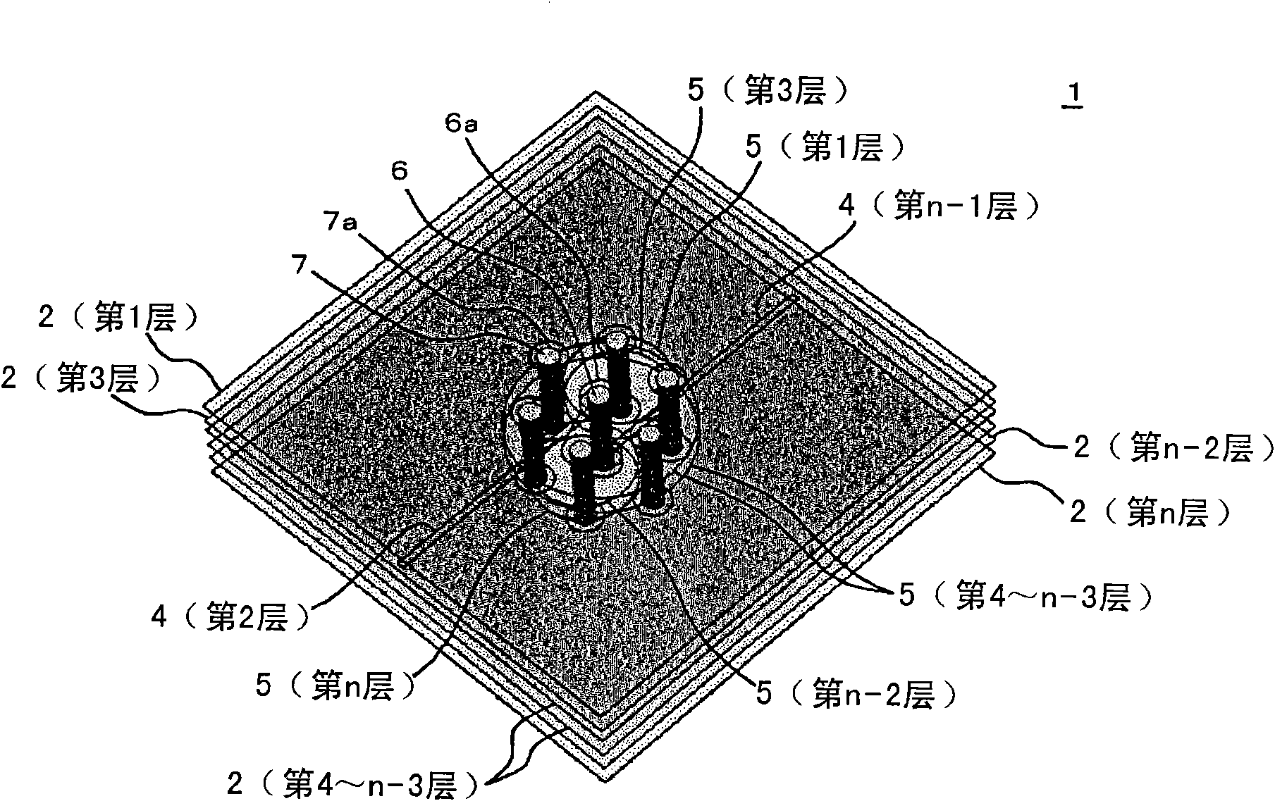
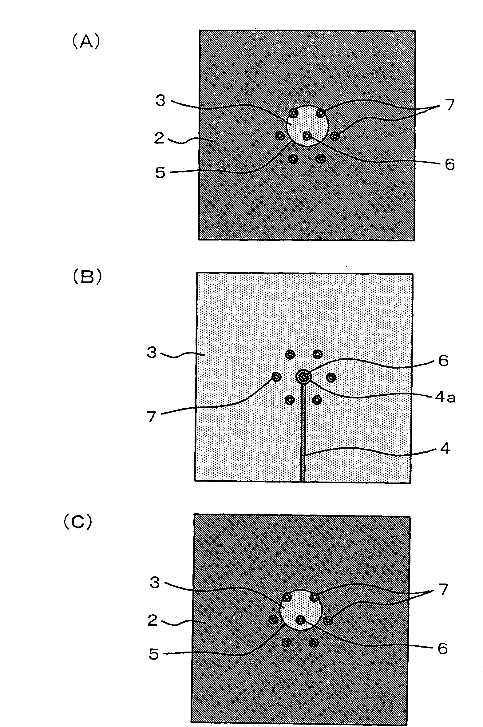
[0030] A printed wiring board according to Embodiment 1 of the present invention will be described with reference to the drawings. figure 1 It is a partial plan view viewed from the first layer side of the GND layer, and schematically shows the structure around the via holes of the printed wiring board according to Example 1 of the present invention. figure 2 It is a partial perspective view showing in outline the structure of the conductor portion around the via hole of the printed wiring board according to the first embodiment of the present invention. image 3 It is a cross-sectional view of (A) the GND layer above the signal wiring, (B) a cross-sectional view of the signal wiring layer, and (C) the signal wiring schematically showing the structure of the printed wiring board according to Embodiment 1 of the present invention. Cross-sectional view of the lower GND layer. Figure 4 It is a cross-sectional view schematically showing the structure of the printed wiring board...

Embodiment 2

[0071] Next, a printed wiring board according to Embodiment 2 of the present invention will be described with reference to the drawings. Figure 9 It is a partial plan view viewed from the first layer side of the GND layer, and schematically shows the structure around the via holes of the printed wiring board according to Example 2 of the present invention.

[0072] In the printed wiring board 1 of the second embodiment, the first-stage upper layer (first layer, n-2th layer) and the first-stage lower layer (the second layer, n-1th layer) of the layer (second layer, n-1th layer) of the signal wiring 4 are arranged The outer shape of the gap 5 of the GND layer 2 of the third layer and the nth layer) is formed as an ellipse (or an oblong shape) that is eccentric with respect to the axis of the via hole 6 for the signal in the following manner, that is, in the slave signal The distance between the signal via hole 6 and the gap 5 in the direction in which the signal wiring 4 is dra...

Embodiment 3

[0074] Next, a printed wiring board according to Embodiment 3 of the present invention will be described with reference to the drawings. Figure 10 It is a partial plan view viewed from the first layer side of the GND layer, and schematically shows the structure around the via holes of the printed wiring board according to Example 3 of the present invention.

[0075] In the printed wiring board 1 of Example 3, the first-stage upper layer (first layer, n-2th layer) and the first-stage lower layer (second layer, n-1th layer) of the layer (second layer, n-1th layer) of the signal wiring 4 are arranged The outer shape of the gap 5 of the GND layer 2 of the third layer and the nth layer) is formed as a quadrilateral (or a polygon) that is eccentric with respect to the center of the axis of the via hole 6 for the signal in the following manner, that is, when the via hole 6 for the slave signal The distance between the signal via hole 6 and the gap 5 in the direction in which the sig...


PUM


Abstract

The present invention relates to a printed wiring board capable of increasing transmission characteristic and a method for manufacturing the same. The printed wiring board comprises: a signal through hole 6; a plurality of GND through holes 7, which are respectively formed at predetermined positions on a circle concentric with the hole for the signal through hole 6; a clearance 5 in the area between the signal through hole and the GND layer 2; and signal wirings 4 which extends from the signal through hole 6 through the clearance between the preset GND layers (such as the first-third layers).The outline of clearance between the upper part and lower part of the signal wiring is formed so that the distance between the through hole 6 and the outline is minimum in a direction in which each of the signal wirings extends from the through hole 6. Further, among the clearances, the outline of each of clearances in the GND layers 2 that are not adjacent to the signal wiring(s) is formed outside a circle established by connecting each center of the GND through holes centering at a center axis of the signal through hole, so that the outline of each of the clearances does not come into contact with the GND through holes.

Description

technical field [0001] The present invention relates to a printed wiring board and its manufacturing method, and more particularly to a printed wiring board having a through hole for high-speed signal transmission and its manufacturing method. Background technique [0002] The improvement in the processing capabilities of communication devices and information devices has been remarkable. In recent years, the frequency of signals transmitted within devices or between devices has been increasing, and there is a possibility that the frequency band of signals on printed wiring boards may be degraded. In particular, the degradation of the signal band at the via hole in the printed wiring substrate of the multilayer wiring structure is fatal to the improvement of the processing capability. Therefore, the following techniques have been proposed as means for reducing signal band degradation in printed wiring boards. [0003] Patent Document 1: Japanese Patent Document Laid-Open No...

Claims


Application Information

Patent Timeline
Patent Type & Authority Applications(China)
IPC IPC(8): H05K1/02H05K1/11H05K3/40H05K3/46
CPCH05K3/429H05K1/116H05K2201/09618H05K1/0222H05K1/0251H05K2201/09718Y10T29/49124Y10T29/49155
Inventor 柏仓和弘
Owner NEC CORP
Why Eureka
Try Eureka