

Wafer supporting glass
A wafer and glass technology, applied in the field of wafer support glass, can solve the problems of inability to be used as wafer support glass, and achieve the effects of reducing defective products and improving impact resistance
- Summary
- Abstract
- Description
- Claims
- Application Information
AI Technical Summary
Problems solved by technology
Method used
Image

Examples
Embodiment approach 1
[0055]
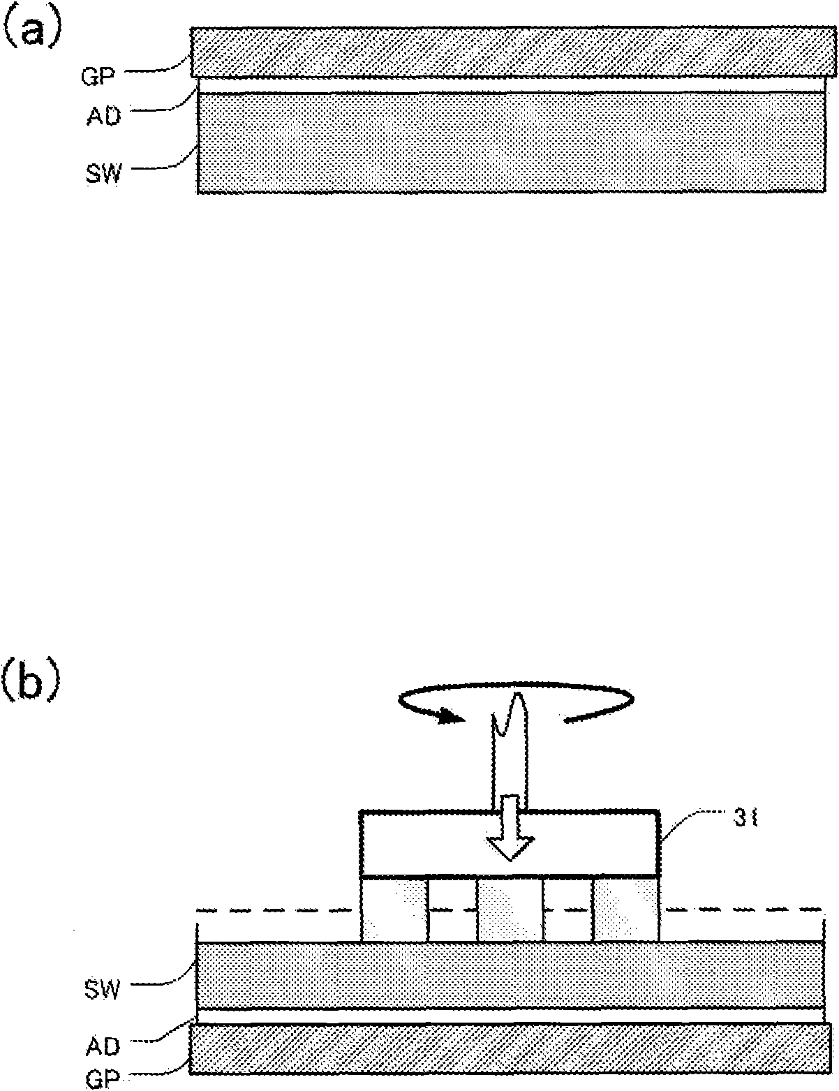
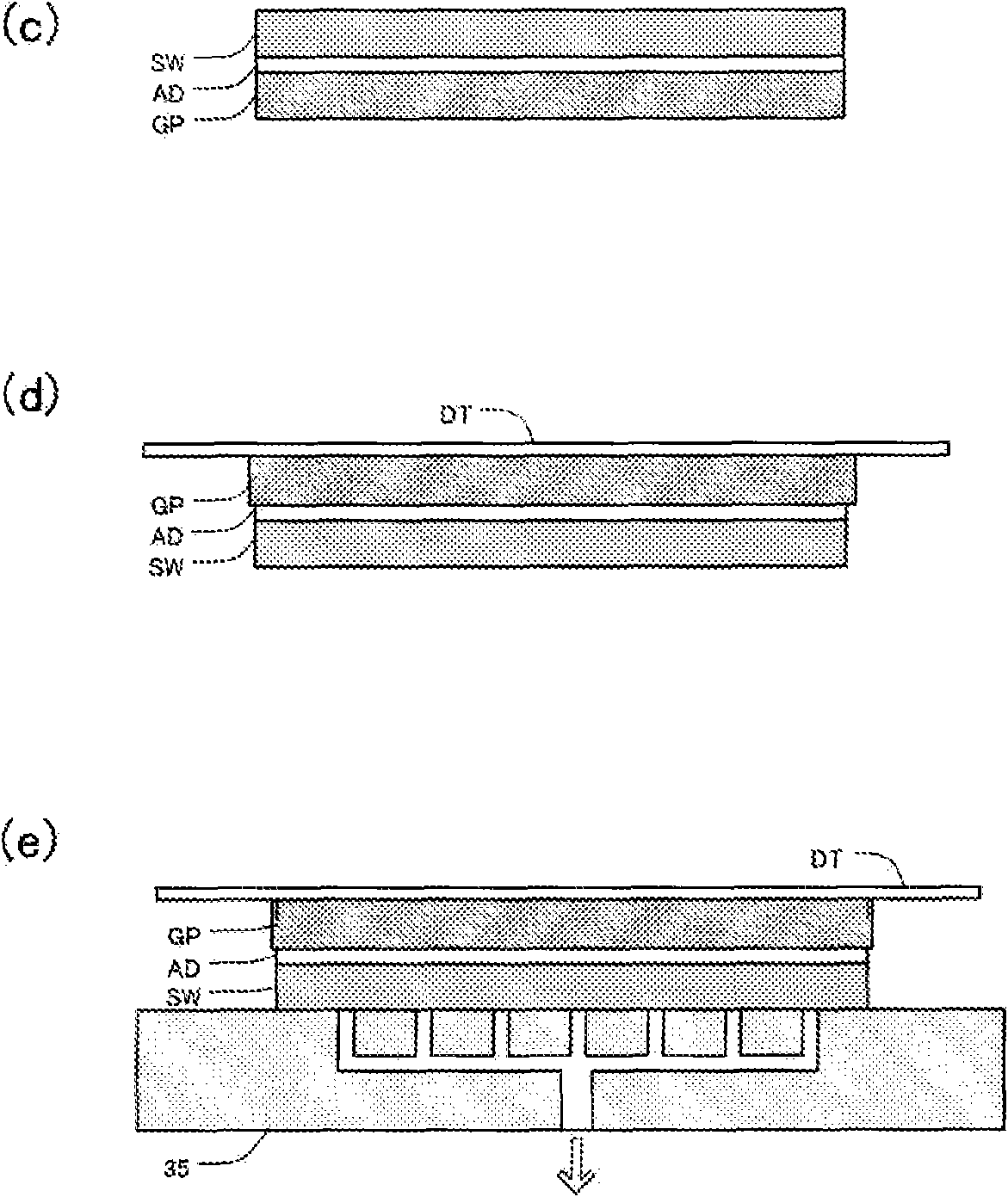
[0056] As described above, by bending the glass plate GP by 30° or more, the glass plate GP can be peeled from the semiconductor wafer SW having the double-sided adhesive film AD without damaging the semiconductor circuit of the semiconductor wafer SW. That is, it is necessary to prepare a glass plate GP that does not crack even when bent by 30° or more. In addition, since the edge portion of the glass plate GP does not come into contact or impact in order to prevent the semiconductor wafer from coming into contact with the wall surface of the stocker or the positioning pins, the edge portion needs to have impact resistance.
[0057] "Glass Substrate"
[0058] Three types of glass substrates were prepared. They were respectively named No. 1 glass, No. 2 glass, and No. 3 glass, and their respective compositions are shown in Table 1. The raw materials used are oxides, carbonates, nitrates and hydroxides.
[0059] (Table 1)
[0060] weight%
SiO 2
...
Embodiment 1
[0072] [Glass Plate GP of Example 1]
[0073] The glass plate GP of Example 1 was produced as follows: First, the glass base material of No. 1 glass was slowly cooled, and then, the shape processing, end surface grinding processing, upper and lower surface grinding processing, end surface grinding processing, and upper and lower surface grinding processing were performed to form A glass-shaped processed object with an outer diameter of 201 mm and a plate thickness of 0.5 mm was manufactured from this. Next, the glass shape processed product was kept at 380°C in KNO 3 (Potassium nitrate): NaNO 3 (Sodium nitrate) = 60%: 40% mixed salt treatment bath immersed for 3 hours. As a result, the Li ions and Na ions on the surface of the glass-shaped processed product are ion-exchanged with the Na ions and K ions in the treatment bath, respectively, and the glass plate GP of Example 1 in which the surface of the glass-shaped processed product is chemically strengthened is obtained. . ...
Embodiment 2
[0074] [Glass Plate GP of Example 2]
[0075] In the same manner as in Example 1, the glass plate GP of Example 2 was produced by slowly cooling the glass base material of No. 1 glass, and then performing contour processing, end surface grinding, upper and lower surface grinding, end surface grinding, and upper and lower surfaces grinding. Processing was performed to form a glass-shaped processed object with an outer diameter of 201 mm and a plate thickness of 0.5 mm, thereby manufacturing it. Next, the glass shape processed product was kept at 380°C in KNO 3 : NaNO 3 =60%: 40% immersion in the treatment bath of mixed salt for 42 hours. That is, the immersion time was extended compared with Example 1, and two kinds of ion exchanges were performed as much as possible, and the glass plate GP of Example 2 was obtained.
PUM
 Abstract
Description
Claims
Application Information