Light emitting device and package assembly for light emitting device

A technology for light-emitting devices and assemblies, applied in the fields of packaging assemblies for light-emitting devices, light-emitting devices, and conductive connecting parts, can solve problems such as adverse effects of light-emitting diodes, and achieve the effects of strong vibration resistance and good heat dissipation

Inactive Publication Date: 2010-03-24
CI KASEI COMPANY
View PDF1 Cites 4 Cited by
  • Summary
  • Abstract
  • Description
  • Claims
  • Application Information

AI Technical Summary

Problems solved by technology

Insufficient temperature control as described above may adversely affect light-emitting diodes in many cases

Method used


Image

  • Light emitting device and package assembly for light emitting device
  • Light emitting device and package assembly for light emitting device
  • Light emitting device and package assembly for light emitting device

Examples


Embodiment 1

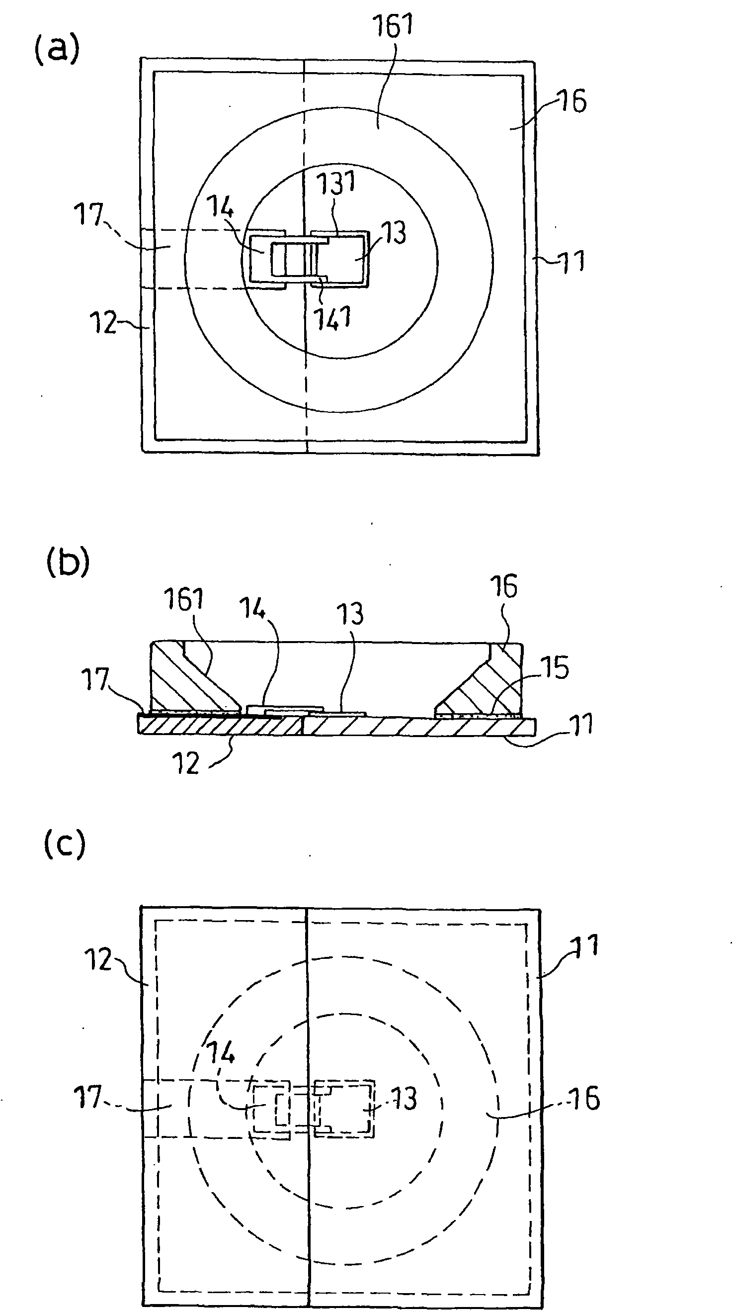
[0049] figure 1 (a)~(c) are embodiment 1 of the present invention, figure 1 (a) is a plan view of the light emitting device, figure 1 (b) is a cross-sectional view of the light emitting device, figure 1 (c) is a bottom view of the light emitting device. In the drawings of the present invention, in order to make the description easier to understand, the magnitude relationship does not necessarily match the actual one. exist figure 1 In (a) to (c), the metal substrate 11 and the ceramic substrate 12 are constituted by a single substrate that is in contact with each other. The reflective frame 16 straddles the metal substrate 11 and the ceramic substrate 12, and integrally fixes the bottom with, for example, a thermosetting resin adhesive.

[0050] The metal substrate 11 is made of, for example, aluminum, copper, iron, or alloys thereof, and is surface-treated with nickel and silver as necessary. The lower electrodes (not shown) of the upper and lower electrode type li...

Embodiment 2

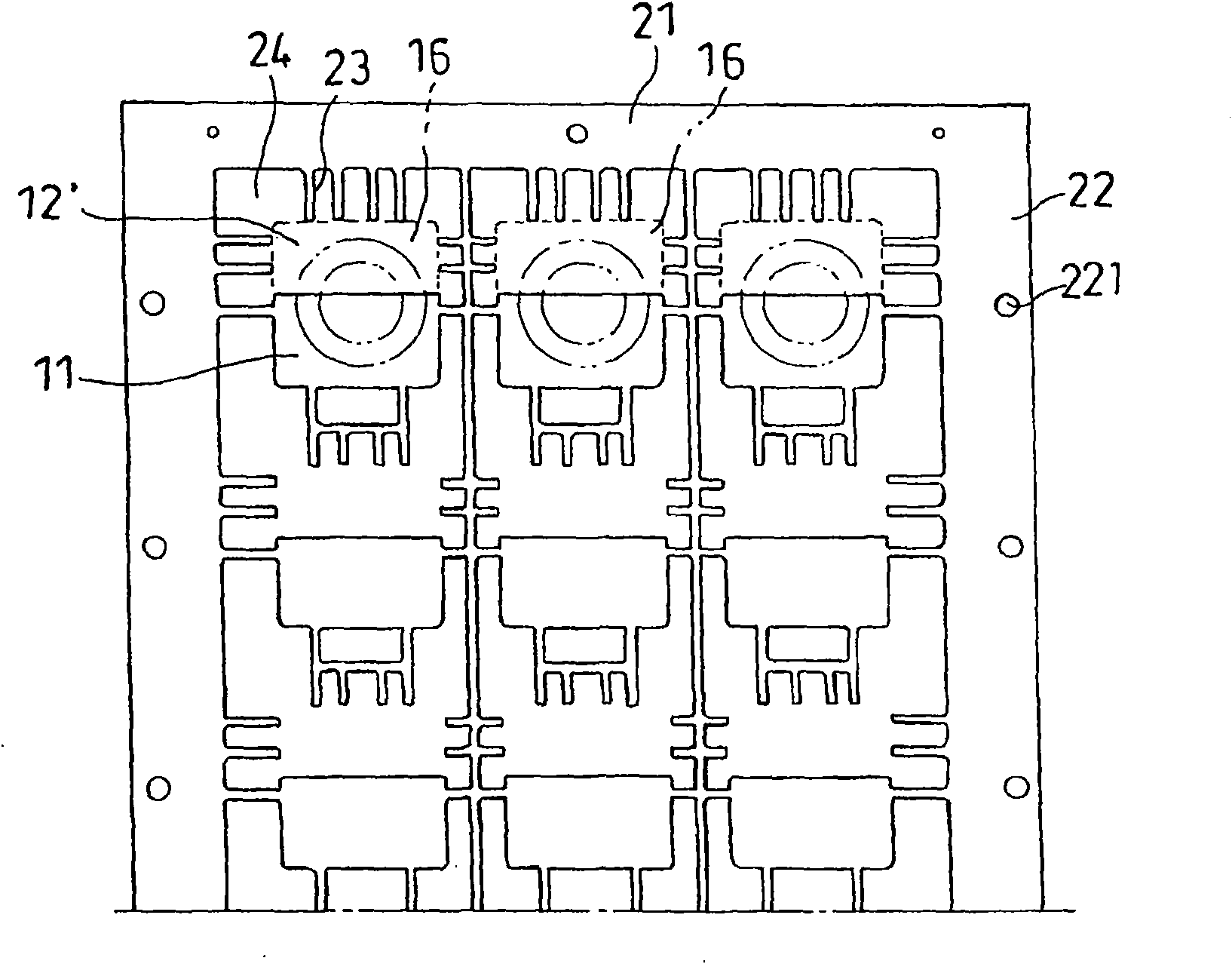
[0058] figure 2 It is a figure for explaining the lead frame provided with the several light emitting diode package connection body. figure 2In the lead frame 21, a plurality of groups of a pair of metal substrates 11 and ceramic substrate fitting holes 12' are connected to the above frame 22 and other metal substrates by using a plurality of lead connection parts 23 composed of weak parts in the frame 22. The substrate 11 or the above-mentioned ceramic substrate fitting holes 12' are connected to form a package connection body. In addition, a plurality of space portions 24 surround the metal substrate 11 and the ceramic substrate fitting hole 12'. The above-mentioned space portion 24 is provided with at least one lead wire connecting portion 23, which is connected to the above-mentioned frame 22, other metal substrate 11 or ceramic substrate fitting hole 12'. In addition, the metal substrate 11 and the ceramic substrate fitting holes 12' may be provided on the frame 22 (l...

Embodiment 3

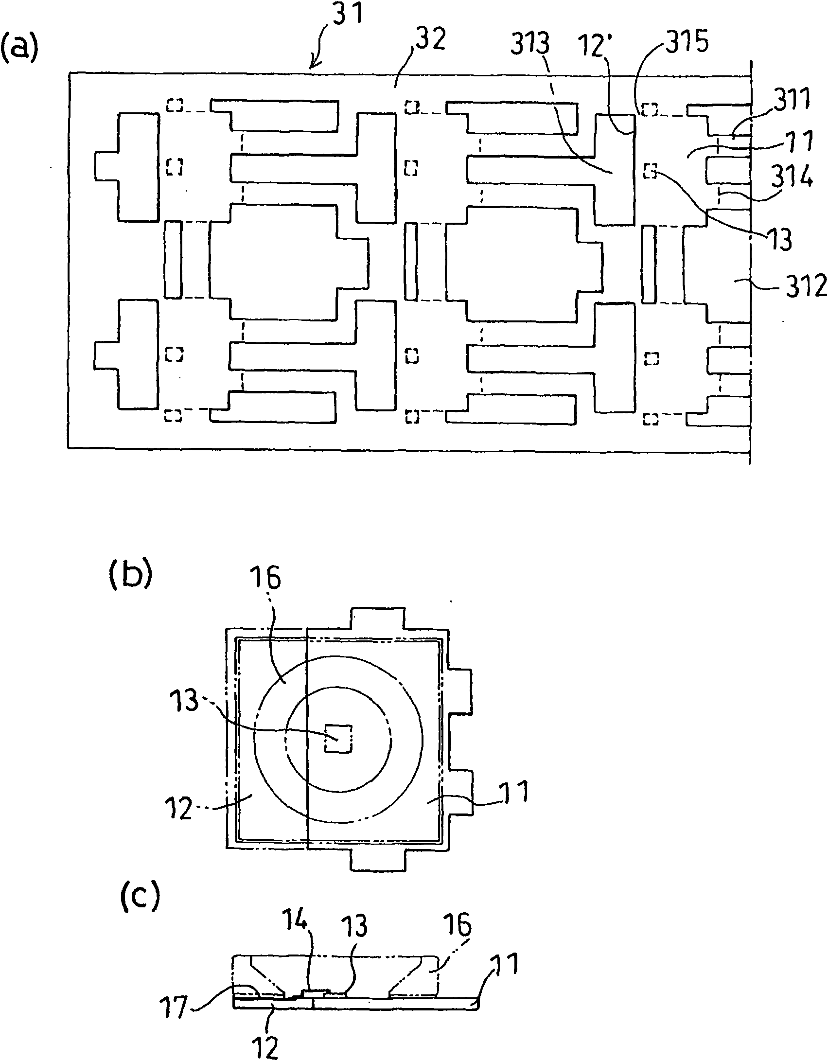
[0061] image 3 (a)-(c) are figures for demonstrating the state where the lead frame provided with the several light emitting diode package connection body, and the upper-lower electrode type light emitting diode were mounted. image 3 In (a), the lead frame 31 is that a plurality of sets of a pair of metal substrates 11 and ceramic substrate fitting holes 12' are connected to the above-mentioned frame 32 and other metal substrates by using a plurality of lead connection parts 311 in the frame 32. 11 or above ceramic substrate fitting hole 12'. In addition, the metal substrate 11 and the ceramic substrate fitting hole 12' are surrounded by a plurality of space portions 312. The above-mentioned space portion 312 is provided with at least one lead wire connecting portion 311, which is connected to the above-mentioned frame 32, other metal substrates 11 or ceramic substrate fitting holes 12'. In addition, the metal substrate 11 and the ceramic substrate fitting holes 12' may be...


PUM

PropertyMeasurementUnit
widthaaaaaaaaaa
thicknessaaaaaaaaaa

Abstract

Provided is a light emitting device having an upper/lower electrode type light emitting diode on a substrate composed of a ceramic board composed of a metal substrate and a ceramic substrate abuttingto the metal substrate. A substrate lead frame for manufacturing the light emitting device is also provided. In the light emitting device, a light emitting section or the like is arranged on a substrate wherein a metal substrate (11) and a ceramic board (12) abut to each other on one side. The ceramic board (12) has a conductive film (17) formed on an upper section. The metal substrate (11) and the ceramic board (12) are bonded with an adhesive such as a thermosetting resin so that a reflection frame (16) composed of an insulating member having an opening section is over the metal substrate and the ceramic board. At least one upper/lower electrode type light emitting diode (13) has a lower electrode on the metal substrate (11). At least one conductive connecting member (14) connects an upper electrode (131) of the upper electrode type light emitting diode (13) and the conductive film (17).

Description

technical field [0001] The present invention relates to a light-emitting device in which upper and lower electrode type light-emitting diodes are provided on a substrate composed of a metal substrate and a ceramic substrate in contact with the metal substrate. The present invention relates to a package assembly for a light-emitting device having the above metal substrate and a ceramic substrate fitting hole for fitting a ceramic substrate in contact with the metal substrate. The present invention relates to a conductive connecting member for connecting the upper electrodes of the upper and lower electrode type light emitting diodes to a conductive film provided on a ceramic substrate. Background technique [0002] Image 6 (a) to (c) are diagrams for explaining conventional examples, and are light emitting devices in which upper and lower electrode type light emitting diodes are provided inside a reflective frame. exist Image 6 In this case, the lower electrodes of the upp...

Claims


Application Information

Patent Timeline
Patent Type & Authority Applications(China)
IPC IPC(8): H01L33/00H01L33/48H01L33/62
CPCH01L33/483H01L33/62H01L24/97H01L2924/01322H01L2924/12041H01L2924/15787H01L2924/351H01L2924/00H01L33/48
Inventor 伏见宏司
Owner CI KASEI COMPANY
Why Eureka
Try Eureka