Test jack for reactive controllable chip

A technology of chip testing and sockets, which is applied to the parts of electrical measuring instruments, measuring electronics, measuring devices, etc., can solve the problems of unsatisfactory reactance, machinability, low price, and increased frequency.

Active Publication Date: 2010-05-19
ANTARES ADVANCED TEST TECH SUZHOU CO LTD
View PDF0 Cites 13 Cited by
  • Summary
  • Abstract
  • Description
  • Claims
  • Application Information

AI Technical Summary

Problems solved by technology

In the existing technology, the main technical measures currently adopted are to shorten the contact probe connecting the chip and the circuit board as much as possible, in an attempt to obtain good high-frequency characteristics, but none of them can meet the requirements of machinability and low price
Similarly, the ch

Method used


Image

  • Test jack for reactive controllable chip
  • Test jack for reactive controllable chip

Examples


Embodiment Construction

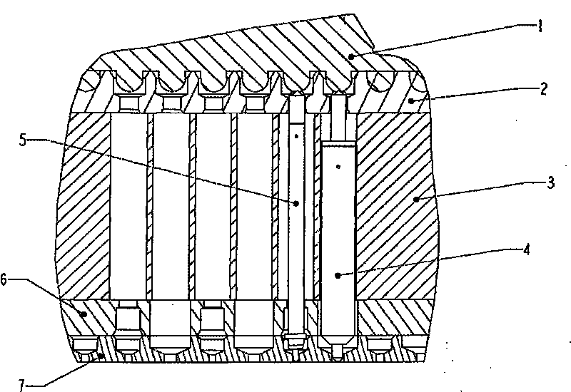
[0007] The technical solutions of the present invention will be further described below in conjunction with the accompanying drawings and embodiments.

[0008] Use screws to fix the chip holding plate 2 and the grounding copper block 3 together, and then select the corresponding probe positioning plate 6 according to the contact distribution of the chip 1, and install the grounding spring probes respectively according to different cavity diameters. Pin 4 and signal / power spring probe 5, then install the probe holding plate 7, and fix it to the socket body with screws, and the entire socket can be assembled.

[0009] The chip holding plate 2 is made of insulating material, and the gaps between all the cavities and the probes 4, 5 are small, so that all the spring probes 4, 5 can be positioned and guided. At the same time, the chip holding plate 2 is also provided with large guide holes to ensure that the balls on the chip 1 are in contact with the spring probe heads 4,5.

[00...


PUM


Abstract

The invention discloses a test jack for a reactive controllable chip, which is composed of a chip holding plate (2), a grounded copper block (3), a probe positioning plate (6), a probe holding plate (7), a ground spring probe (4) and a signal/power supply spring probe (5). With the increasing running speed of integrated circuit chips, a chip test fixture which can meet the demand of test industry should include better high-frequency integrated signal so that reactance (impedance) thereof is within a certain range to reduce the loss of electric signals at the time of get-through. Meanwhile, according to the invention, use requirements can be satisfied only by conveniently replacing the probe positioning plate (6) instead of changing other parts when the distribution of contacts using different chips (1) is changed, thus greatly enhancing the processability of the test jack and lowering cost.

Description

technical field [0001] The invention belongs to the semiconductor industry, in particular to a testing device for semiconductor chips. Background technique [0002] With the increasing operating speed of integrated circuit chips, the chip testing industry requires chip test fixtures to have higher high-frequency signal integration performance. In the actual test of the chip, the test fixture must maintain the reactance (or impedance) within a certain range (for example, 50 ohms), so as to reduce the loss caused by the electrical signal passing through. However, none of the current chip test fixtures can meet the high requirements. frequency requirements. According to retrieval, before the present invention was made, no reactance controllable chip test socket identical to the present invention has been found. In the prior art, the main technical measure adopted at present is to shorten the contact probe connecting the chip and the circuit board as much as possible in an att...

Claims


Application Information

Patent Timeline
IPC IPC(8): H01R13/24H01R13/42H01R13/648G01R1/04G01R1/073
Inventor 陶西昂潘杰姆周家春杨晓勇
Owner ANTARES ADVANCED TEST TECH SUZHOU CO LTD
Why Eureka
Try Eureka