Co-electrode thin SOI longitudinal bipolar transistor device and manufacturing method thereof

A technology of bipolar transistors and manufacturing methods, applied in semiconductor/solid-state device manufacturing, electric solid-state devices, semiconductor devices, etc., can solve problems such as low integration, low operating current, and large inter-electrode capacitance, and reduce process complexity degree, increase the working current, improve the effect of frequency performance

Active Publication Date: 2010-06-02
SHANGHAI HUAHONG GRACE SEMICON MFG CORP
View PDF0 Cites 2 Cited by
  • Summary
  • Abstract
  • Description
  • Claims
  • Application Information

AI Technical Summary

Problems solved by technology

[0008] like figure 1 The disadvantages of the prior art shown include the following points: ①. The transistors do not share any electrodes, resulting in a non-compact structure and low integration. In addition, the operating current is low and the input impedance matching is difficult during use; ②. Two ion implantation processes are used to form the base connection region 41 and the base lead-out region 42 respectively. The process is complicated. In addition, the ion implantation alignment accuracy of the base connection region 41 is required to be high, which further aggravates the process complexity; ③, the base The current flows along the edge of the second isolation structure 22 through the base connection region 41 to the base lead-out region 42 and is led out therefrom, resulting in a larger resistance of the base path, that is, the base input resistance Rb, thereby reducing the current Ib and the frequency of the BJT performance; ④, the base connection region 41 is in contact with the collector region 30 and the silicon emitter region 50, and the collector region 30 is in contact with the silicon base region 40 and the base connection region 41, resulting in the base, the emitter and the collector The inter-electrode capacitance between electrodes is large, which affects the frequency performance of SOI bipolar transistor devices

Method used


Image

  • Co-electrode thin SOI longitudinal bipolar transistor device and manufacturing method thereof
  • Co-electrode thin SOI longitudinal bipolar transistor device and manufacturing method thereof
  • Co-electrode thin SOI longitudinal bipolar transistor device and manufacturing method thereof

Examples


Embodiment Construction

[0027] The common electrode thin SOI vertical bipolar transistor device and its manufacturing method of the present invention will be further described in detail below.

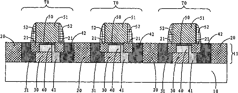
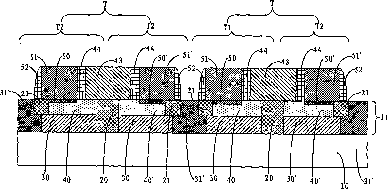
[0028] see figure 2 , which shows the composition structure of the common electrode thin SOI vertical bipolar transistor device of the present invention, as shown in the figure, the common electrode thin SOI vertical bipolar transistor device is fabricated in the top layer silicon 11, including a plurality of transistor units T , each transistor unit T includes first and second transistors T1 and T2 of the same type, the top layer silicon 11 is fabricated on the insulating buried layer 10, the top layer silicon 11 has first and second isolation structures 20 and 21, the insulating buried layer Below 10 is a silicon substrate (not shown), and the insulating buried layer 10 is usually silicon oxide. The first isolation structure 20 is a shallow trench isolation structure (STI), and the second isolation struct...


PUM


Abstract

The invention provides a co-electrode thin SOI longitudinal bipolar transistor device and a manufacturing method thereof. In the prior art, the transistors does not share an electrode so as to cause incompact device structure and low integration degree, and in addition, the base leading-out area is connected with the silicon base area through the base connecting area so as to cause complex process, high base input resistance and poor frequency performance. The device of the invention comprises a plurality of transistor units provided with first and second transistors; both the first and second transistors have a collector area, a silicon base area and a silicon emitter area which are overlapped in the top silicon in turn and a polycrystalline emitter area arranged on the top silicon; a shared polycrystalline base area is connected with the silicon base areas of the first and second transistors, arranged between the polycrystalline emitter areas of the first and second transistors, and isolated with the polycrystalline emitter areas through a medium isolation structure; and a shared collector leading-out area is arranged between two adjacent transistor units, and two ends of the shared collector leading-out area are connected with the collector areas at two sides respectively. The device has the advantages of compact structure, high integration degree, low base input resistance and good frequency performance.

Description

technical field [0001] The invention relates to the field of bipolar transistors, in particular to a common electrode thin SOI vertical bipolar transistor device and a manufacturing method thereof. Background technique [0002] As the feature size of integrated circuits continues to decrease and enter the nanometer stage, the existing bulk silicon materials and processes are approaching their physical limits. To further improve the integration and operating speed of integrated circuits, it is necessary to improve materials and processes There are new major breakthroughs. Silicon on Insulator (Silicon On Insulator; SOI for short) is a major breakthrough in materials at present. It is recognized by the industry as one of the solutions to replace the existing monocrystalline silicon materials in the era of nanotechnology, and it is a major factor in maintaining the trend of Moore's Law. weapon. [0003] SOI has a three-layer structure of "top silicon-insulating buried layer-s...

Claims


Application Information

Patent Timeline
Patent Type & Authority Applications(China)
IPC IPC(8): H01L27/12H01L21/84
Inventor 周建华陈天兵彭树根高明辉
Owner SHANGHAI HUAHONG GRACE SEMICON MFG CORP
Why Eureka
Try Eureka