Image sensing device

A technology of image sensing and sensing electrodes, which is applied in the field of image sensing devices, can solve the problems of reducing sensing sensitivity and small sensing capacitance, so as to increase the ability to resist electrostatic damage, increase the ability to resist impact damage, increase effect of thickness

Active Publication Date: 2010-06-09
EGIS TECH
View PDF0 Cites 13 Cited by
  • Summary
  • Abstract
  • Description
  • Claims
  • Application Information

AI Technical Summary

Problems solved by technology

However, too thick protective layer will result in a small sensing

Method used


Image

  • Image sensing device
  • Image sensing device
  • Image sensing device

Examples


Embodiment Construction

[0044] In order to make the above content of the present invention more comprehensible, a preferred embodiment will be described in detail below with the accompanying drawings.

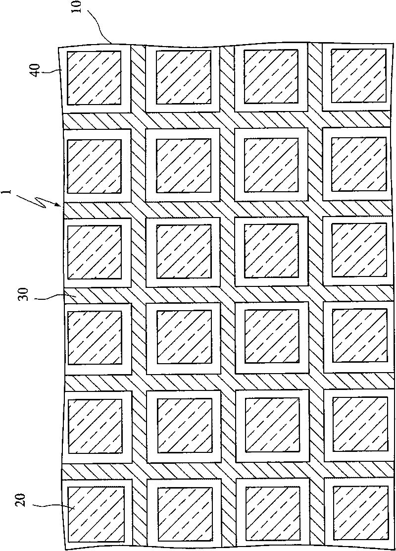
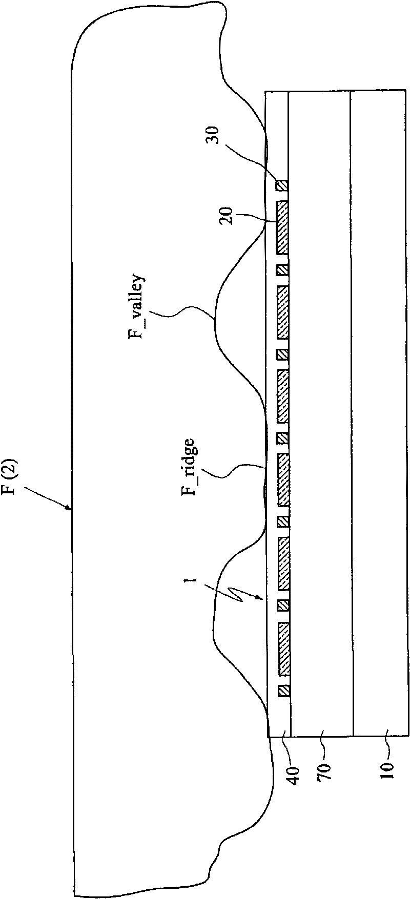
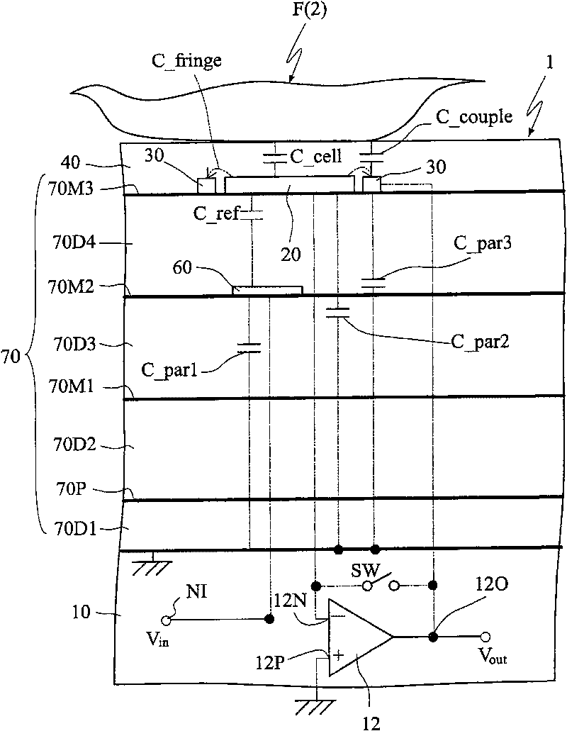
[0045] figure 1 A schematic top view showing a part of the sensing element array of the sensing device 1 of the present invention. figure 2 It is a schematic diagram of the sensing device of the present invention in a state of use. image 3 It is an enlarged cross-sectional schematic diagram showing a single sensing element according to the first embodiment of the present invention. Such as Figure 1 to Figure 3 As shown, the image sensing device 1 of this embodiment is used to sense an image of an object 2 . The image sensing device 1 at least includes a negative feedback amplifier 12 , a substrate 10 , a sensing electrode 20 , a coupling electrode 30 and an insulating protection layer 40 .

[0046] The material of the substrate 10 is a silicon material in the present invention, and may also be ...


PUM


Abstract

The invention relates to an image sensing device which is used for sensing an image of an object. The image sensing device at least comprises a negative feedback amplifier, a substrate, a sensing electrode, a coupling electrode and an insulation protection layer, wherein the sensing electrode and the coupling electrode are arranged above the substrate; the insulation protection layer covers the sensing electrode and the coupling electrode; the sensing electrode and the object form a sensing capacitor; the coupling electrode and the object form a coupling capacitor; a negative input end of the negative feedback amplifier is electrically connected with the sensing electrode; and the coupling electrode is electrically connected to a signal output end of the negative feedback amplifier or a signal input end of the image sensing device.

Description

technical field [0001] The invention relates to an image sensing device, in particular to an image sensing device for sensing skin texture. Background technique [0002] The capacitive sensing technology applied to human skin is known, and can be applied, for example, to a fingerprint sensor for sensing fingerprint paths or as a touch panel or screen for capacitive touch. [0003] Especially as a skin texture sensor, the basic structure of the part in contact with the skin texture is an array-type sensing element, that is, a two-dimensional sensor is composed of several identical sensing elements, such as finger placement When on it, the fingerprint pattern has ridges and valleys, the ridges are in direct contact with the sensor, and the ridges are separated from the sensor by a gap, passing through each sensing element or contacting the valleys. The contact of the peaks or the formation of gaps with the valleys can capture the fingerprint path in the two-dimensional capaci...

Claims


Application Information

Patent Timeline
IPC IPC(8): G06K9/00G06K9/20A61B5/117A61B5/00
Inventor 周正三
Owner EGIS TECH
Why Eureka
Try Eureka