

Active component array substrate and detection method thereof
An array substrate and active element technology, which is applied in the field of active element array substrate and its detection, can solve the problems of electrostatic breakdown, inconvenience, and general products and methods do not have suitable structures and methods, so as to avoid electrostatic damage and improve circuit performance. The effect of stability
- Summary
- Abstract
- Description
- Claims
- Application Information
AI Technical Summary
Problems solved by technology
Method used
Image

Examples
Embodiment Construction
[0042] In order to further explain the technical means and effects of the present invention to achieve the intended purpose of the invention, the specific implementation, structure, The detection method, steps, features and efficacy are described in detail below.
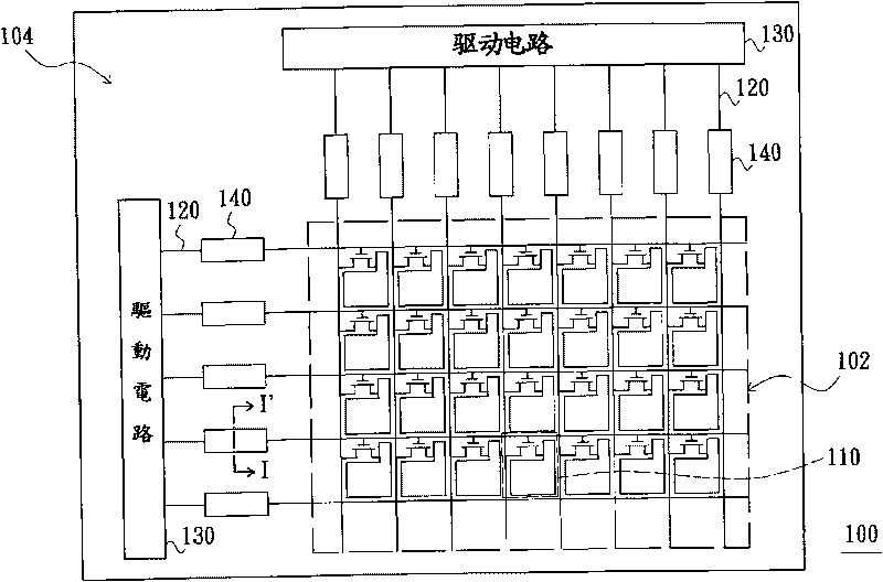
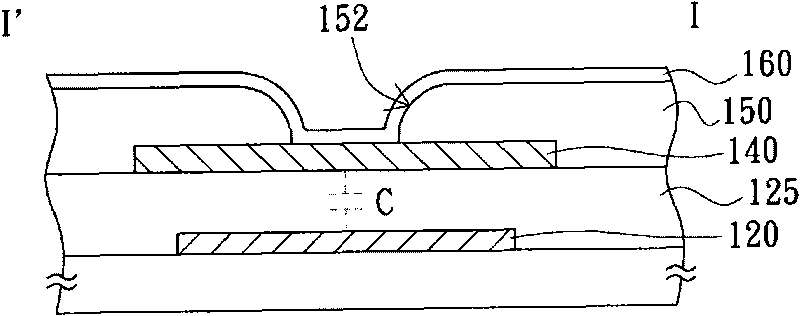
[0043] see image 3 and Figure 4 , image 3 is a schematic diagram of an embodiment of the active element array substrate of the present invention, Figure 4 Then, it is a schematic cross-sectional view of the active device array substrate in an embodiment of the present invention where the detection pads are disposed. The active device array substrate 300 in an embodiment of the present invention has a display area 302 and a peripheral circuit area 304, and the active device array substrate 300 includes a plurality of pixel units 310, a plurality of signal wires 320, a plurality of detection pads 330 and a first interposer. electrical layer 340 .
[0044] The aforementioned pixel units 310 are arranged in the...
PUM
 Abstract
Description
Claims
Application Information