Bug repairing apparatus

A defect repairing and installation technology, which is applied in the field of defect repairing devices, can solve problems such as optical fiber deformation, inability to process substrates, and reduced durability, and achieve the effect of a relatively short distance

A defect repairing and installation technology, which is applied in the field of defect repairing devices, can solve problems such as optical fiber deformation, inability to process substrates, and reduced durability, and achieve the effect of a relatively short distance

CN101733545AInactive Publication Date: 2010-06-16OLYMPUS CORP

Image

  • Bug repairing apparatus
  • Bug repairing apparatus
  • Bug repairing apparatus

Examples


Embodiment Construction

[0045] Hereinafter, a defect repairing device according to an embodiment of the present invention will be described with reference to the drawings.

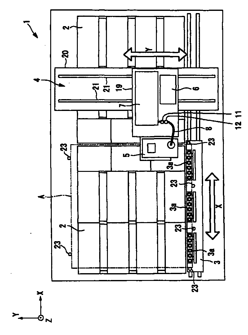
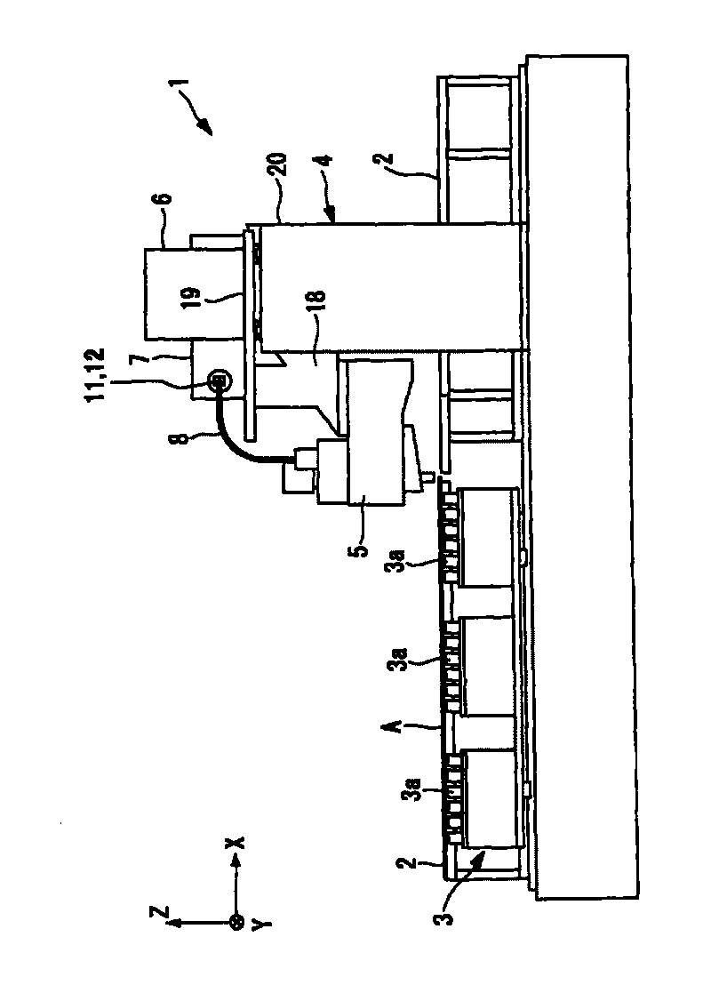
[0046] Figure 1A and Figure 1B It is a top view and a front view which show the defect repairing apparatus 1 which concerns on one Embodiment of this invention.

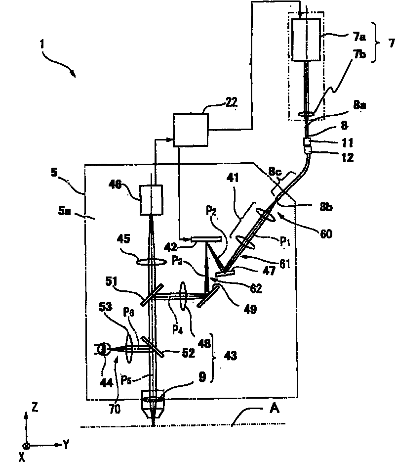
[0047] figure 2 It is a schematic structural diagram for explaining the internal structure of the processing head 5 of the defect repairing apparatus 1.

[0048] Figure 3A and Figure 3B It is a schematic side view and a schematic front view for explaining the optical fiber 8 and the mode scramblers 11 and 12 of the defect repairing device 1 .

[0049] The defect repairing device 1 is used, for example, for detecting a short circuit in a wiring portion, photoresist leakage, etc., in a glass substrate A on which a circuit pattern is formed by a photolithography process step in a manufacturing process of an FPD such as a liquid crystal display (LCD). When there a...


PUM

PropertyMeasurementUnit
lengthaaaaaaaaaa

Abstract

The present invention provides a bug repairing apparatus which irradiates laser lights distributed uniformly on a base plate. The bug repairing apparatus leads laser lights emitted from a laser light source to a processing head to repair the bug part on the base plate. The bug repairing apparatus comprises a base platform which maintain a base plate at a flat state, a portal type rack constructed isolating from the base platform, a driving mechanism which make the base platform and the rack move relatively, an installation part capable of moving along the rack and a horizontal beam, and the laser light source and the processing head being in integrated installation with the installation part, an optical fiber for connecting the laser light source and the processing head that are integrally installed on the installation part, and a plurality of mode scramblers for bending the optical fiber to different directions slightly to adjust mode distribution in the optical fiber.

Description

technical field [0001] The present invention relates to a defect repairing device for repairing defects of substrates such as flat panel displays (FPDs) and semiconductor wafers with laser light. Background technique [0002] Conventionally, there has been a method of repairing defects in the substrate by irradiating the substrate with laser light emitted from a laser light source using a processing head. As an apparatus for repairing such defects, for example, a laser processing apparatus in which a laser oscillator and a processing head are connected by an optical fiber is known (see Patent Document 1). [0003] The laser processing device described in the above-mentioned Patent Document 1 has: a laser oscillator fixed at the end of the device; between. [0004] Patent Document 1: Japanese Patent Application Laid-Open No. 9-239578 [0005] However, since the laser processing apparatus described in the aforementioned Patent Document 1 moves only the laser oscillator and ...

Claims


Application Information

Patent Timeline
16 Jun 2010
Publication
CN101733545A
IPC
B23K26/00; B23P6/00
CPC
B23K26/062; B23K26/0648; B23K26/10; G02F1/1309
Inventors
中村达哉; 赤羽隆之