
Silicon micro-acceleration sensor chip

An acceleration sensor and chip technology, applied in the direction of acceleration measurement using inertial force, can solve the problems of low sensitivity, large weight, low frequency response, etc., and achieve the effect of high sensitivity, small weight and high frequency response

Inactive Publication Date: 2010-06-16
XI AN JIAOTONG UNIV
View PDF0 Cites 16 Cited by
  • Summary
  • Abstract
  • Description
  • Claims
  • Application Information

AI Technical Summary

Problems solved by technology

For those acceleration sensors with a large range such as tens of thousands of g, due to their large sensitive structure stiffness, they can reach hundreds of KHz, but the output per unit acceleration is small and the sensitivity is low, so they cannot be used in the measurement of small accelerations; at the same time, for those small ranges such as Acceleration sensors with hundreds to thousands of g, due to their soft sensitive structure, although the unit acceleration output is large, because of their low response frequency, it brings difficulties to dynamic measurement
In short, the existing acceleration sensors have the disadvantages of large volume, heavy weight, low frequency response and low sensitivity

Method used


Image

  • Silicon micro-acceleration sensor chip
  • Silicon micro-acceleration sensor chip
  • Silicon micro-acceleration sensor chip

Examples


Embodiment Construction

[0017] The structure and working principle of the present invention will be described in detail below in conjunction with the accompanying drawings.

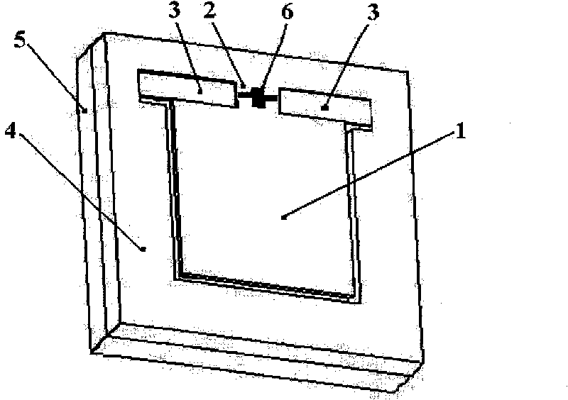
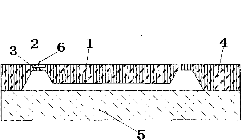
[0018] see figure 1 , 2 , 3, 4, a silicon micro-acceleration sensor chip, including a peripheral supporting silicon base 4, a glass substrate 5 is arranged on the back side of the peripheral supporting silicon base 4, and the back side of the peripheral supporting silicon base 4 is bonded to the glass substrate 5 connection, the central silicon mass 1 is located in the middle of the peripheral supporting silicon base 4, two silicon membranes 3 are arranged on the front side of the peripheral supporting silicon base 4 and the adjacent side of the central silicon mass 1, and the two silicon membranes 3 One side is connected with the peripheral supporting silicon base 4 and the central silicon mass 1, and the other side is connected with the silicon cantilever beam 2 to form a beam-membrane structure to jointly support the central...


PUM


Abstract

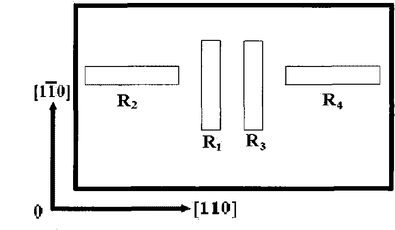
The invention discloses a silicon micro-acceleration sensor chip, which comprises a central silicon mass block which is positioned in the center of a peripheral support silicon substrate; two silicon films are arranged at two ends of one side of the front of the peripheral support silicon substrate adjacent to the central silicon mass block; one surface of one silicon film and one surface of the other silicon film are connected with the peripheral support silicon substrate and the central silicon mass block, while the other surfaces are connected with a silicon cantilever; the middle of the silicon cantilever is provided with four piezoresistive strips so as to form a Wheatstone bridge; when acceleration is acted on the sensor chip, inertia force is acted on the central mass block to deform the cantilever-film structure, the resistance of the piezoresistive strips is changed under the stress action of the silicon cantilever, the Wheatstone bridge loses balance and outputs an electric signal corresponding to the external acceleration so as to measure the acceleration by the sensor chip. The silicon micro-acceleration sensor chip has the advantages of small volume, light weight, high frequency response and high sensitivity.

Description

technical field [0001] The invention belongs to the technical field of micro-mechanical electronics, and in particular relates to a silicon micro-acceleration sensor chip. Background technique [0002] At present, the high-performance acceleration sensor for dynamic measurement has become one of the important application fields of the acceleration sensor. The impact acceleration sensor of the automobile industry and the spindle acceleration sensor of the high-speed machine tool have put forward high requirements on the acceleration sensor in terms of sensitivity and response frequency. Require. In the design of sensors for such applications, the static sensitivity and dynamic response frequency of the sensor are two equally important parameters, both of which must meet certain requirements in order to achieve accurate measurement of the specific measured acceleration. According to the existing acceleration sensor using the traditional cantilever beam structure, it can be kn...

Claims


Application Information

Patent Timeline
Patent Type & Authority Applications(China)
IPC IPC(8): G01P15/12
Inventor 赵玉龙刘岩田边张玲蒋庄德
Owner XI AN JIAOTONG UNIV
Learn More