Encapsulation structure for wafer backside

A technology of packaging structure and crystal back, which is applied in the direction of electrical components, electrical solid devices, circuits, etc., can solve the problem of increasing the process cost of depositing silicon dioxide layer, and achieve the effect of promoting gettering effect, saving process cost and preventing automatic doping Effect

Inactive Publication Date: 2010-06-16
WAFER WORKS
View PDF4 Cites 23 Cited by
  • Summary
  • Abstract
  • Description
  • Claims
  • Application Information

AI Technical Summary

Problems solved by technology

[0019] However, if the dopant is worried about diffusing out from the wafer, the thickness of the silicon dioxide layer must be increased to completely prevent the dopant from seeping out, so the process cost of depositing the silicon dioxide layer will inevitably increase

Method used


Image

  • Encapsulation structure for wafer backside
  • Encapsulation structure for wafer backside
  • Encapsulation structure for wafer backside

Examples


no. 1 example

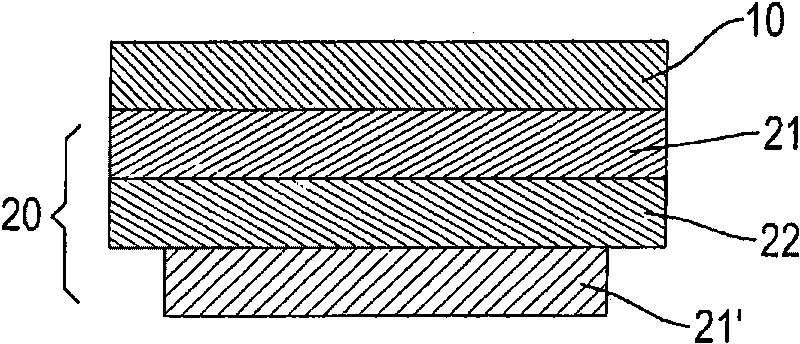
[0043] Please see figure 1 Shown is the first embodiment of the packaging structure of the crystal back of the present invention, which includes:

[0044] A semiconductor substrate 10, which can be silicon, germanium or other semiconductors, the bottom of which can first undergo backside damage (BSD), which uses mechanical force to damage the crystal back to achieve the effect of removing impurities. For the method, reference may be made to US Patent No. 5,006,475, US Patent No. 5,066,359 and China Taiwan Publication No. 200820332 "Silicon Wafer with High Gettering Capability and High Flatness and Manufacturing Method thereof".

[0045] A multi-layer structure layer 20, which comprises two layers of silicon dioxide layers 21, 21' and a polysilicon layer 22 arranged between said silicon dioxide layers 21, 21', wherein a silicon dioxide layer 21 is directly arranged At the bottom of the semiconductor substrate 10, the polysilicon layer 22 is disposed on a surface of the silicon...

no. 2 example

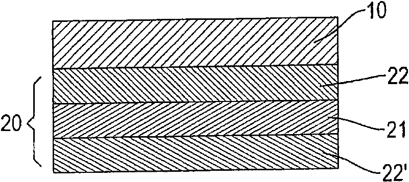
[0047] Please see figure 2 Shown is the second embodiment of the packaging structure of the crystal back of the present invention, which includes:

[0048] A semiconductor substrate 10, which can be silicon, germanium or other semiconductors, the bottom of which can first undergo backside damage (BSD), which uses mechanical force to damage the crystal back to achieve the effect of removing impurities. For the method, reference may be made to US Patent No. 5,006,475 and Taiwan Patent Publication No. 200820332 "Silicon Wafer with High Gettering Capability and High Flatness and Manufacturing Method thereof".

[0049] A multi-layer structure layer 20 includes two layers of polysilicon layers 22, 22' and a silicon dioxide layer 21 disposed between the polysilicon layers 22, 22', wherein a polysilicon layer 22 is directly disposed on the semiconductor substrate 10 At the bottom, the silicon dioxide layer 21 is disposed on a surface of the polysilicon layer 22 different from the se...


PUM


Abstract

The invention relates to an encapsulation structure for wafer backside. The structure comprises a semiconductor substrate and a multilayered structural layer which is arranged at the bottom of the semiconductor substrate and is formed by combining a polysilicon layer and an insulating layer (such as a silicon dioxide layer); the multilayered structure can promote the effect of impurity absorption, effectively prevents automatic doping, improves the phenomenon of burr, and saves process cost; and through the structure, the bowing degree and the warping degree of the silicon substrate are easily adjusted.

Description

technical field [0001] The present invention relates to a packaging structure of a crystal back, especially a kind of one that can effectively improve the problems of auto-doping and silicon nodule generated during epitaxial growth, and can save costs The packaging structure of wafer backside. Background technique [0002] A general semiconductor process may include the following steps: [0003] 1. Single crystal growth (crystal growth), usually grows a single crystal silicon rod without dislocation defects by the Czochralski method (CZ). Single crystals are divided into P-type single crystals and N-type single crystals. P Type single crystal is doped with group IIIA elements (such as boron), while N-type single crystal is doped with group VA elements (such as phosphorus, arsenic, or antimony); [0004] 2. Slicing refers to cutting the above-mentioned monocrystalline silicon rod into sliced ​​wafers with a slicer, and the slicing technique will affect the warpage of the wa...

Claims


Application Information

Patent Timeline
Patent Type & Authority Applications(China)
IPC IPC(8): H01L23/00
Inventor 吴俊泰邱恒德
Owner WAFER WORKS
Why Eureka
Try Eureka