Almost perfect absorbing structure for wide wave band
A near-perfect absorption and wide-band technology, which is applied in the field of electromagnetic wave absorption structures, can solve the problems that the positive effect of near-perfect absorption has not been proposed, and achieve the effects of easy processing, excellent absorption bandwidth and efficiency, and expansion of absorption bandwidth
- Summary
- Abstract
- Description
- Claims
- Application Information
AI Technical Summary
Problems solved by technology
Method used
Image
Examples
Embodiment
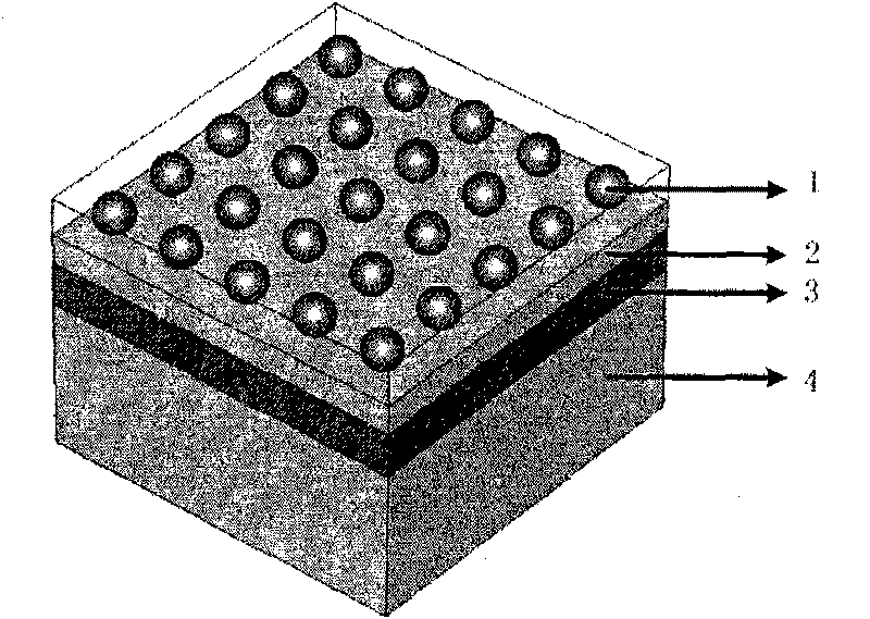
[0026] A fabrication process of a near-perfect absorption structure for broadband electromagnetic waves using a periodic metal nanosphere array is as follows:
[0027] (1) Select the visible light band, the dielectric absorbing material selects polymer solar cell photosensitive material P3HT:PCBM, and its absorption range is 350nm-630nm; the metal material selects silver and aluminum;
[0028] (2) Fabrication of the device structure: a. Utilize metal aluminum to vapor-deposit a metal film with a thickness greater than 1m on the quartz base material, so that electromagnetic waves cannot be transmitted; b. Spin-coat a 100nm thick absorption medium material on the metal film; c. Using micro-processing technology, such as self-assembly technology, to make silver metal nanosphere particles on the absorption medium layer;
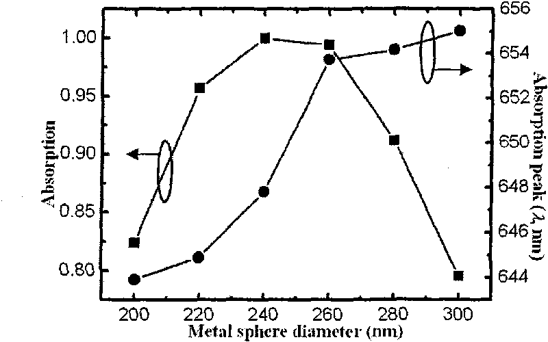
[0029] (3) The minimum wavelength of visible light is 400nm, so the diameter d of the metal ball particles is less than 400nm;
[0030] (4) Broad-band near-perf...
PUM
 Abstract
Description
Claims
Application Information


