Almost perfect absorbing structure for wide wave band

A near-perfect absorption and wide-band technology, which is applied in the field of electromagnetic wave absorption structures, can solve the problems that the positive effect of near-perfect absorption has not been proposed, and achieve the effects of easy processing, expanded absorption bandwidth, excellent absorption bandwidth and efficiency

Inactive Publication Date: 2013-01-02
INST OF OPTICS & ELECTRONICS - CHINESE ACAD OF SCI
View PDF0 Cites 4 Cited by
  • Summary
  • Abstract
  • Description
  • Claims
  • Application Information

AI Technical Summary

Problems solved by technology

But no positive role for near-perfect absorption has been suggested in metal particle-based solar cell research

Method used


Image

  • Almost perfect absorbing structure for wide wave band
  • Almost perfect absorbing structure for wide wave band
  • Almost perfect absorbing structure for wide wave band

Examples


Embodiment

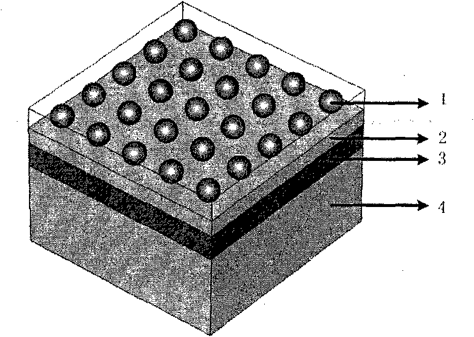
[0026] The fabrication process of a near-perfect absorption structure for broadband electromagnetic waves using periodic metal nanosphere arrays is as follows:

[0027] (1) Select the visible light band, the dielectric absorption material selects the polymer solar cell photosensitive material P3HT:PCBM, and its absorption range is 350nm-630nm; the metal material selects silver and aluminum;

[0028] (2) Fabrication of device structure: a. Use metal aluminum to vapor-deposit a metal film with a thickness of more than 1 m on the quartz base material, so that electromagnetic waves cannot be transmitted; b. Spin-coat a 100-nm-thick absorption dielectric material on the metal film; c. Using microfabrication technology, such as self-assembly technology, to make silver metal nanospheres on the absorption medium layer;

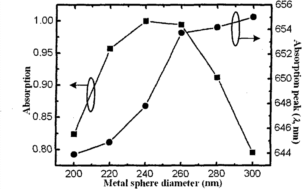
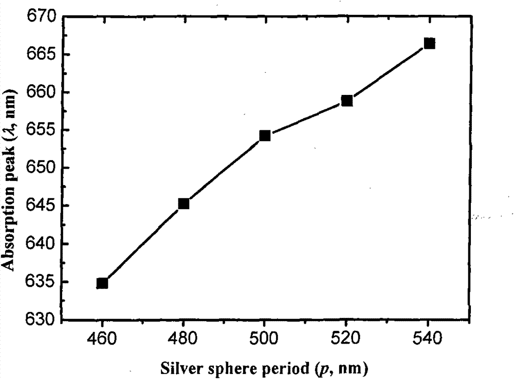
[0029] (3) The minimum wavelength of visible light is 400nm, so the diameter d of the metal spherical particles is less than 400nm;

[0030] (4) Broad-band near-perf...


PUM


Abstract

The invention relates to an almost perfect absorbing structure for wide wave band, which comprises the following steps: (1) determining absorbing material and metal material according to the incoming wave frequency band; (2) manufacturing structure of apparatus; (3) determining the range of diameter d of metal spherical particles according to the local effect of plasma on the surface of the metalspherical particles; (4) determining the distribution and range of period p according to the electromagnetic resonation effect among metal spherical particles-medium-metal film; and (5) optimizing particle diameter d and distribution period p to realize expansion of the bandwidth of the entire apparatus. The invention realizes almost perfect absorbing function on wide wave band within visible light range.

Description

technical field [0001] The invention relates to an electromagnetic wave absorption structure, in particular to a new type of electromagnetic wave near-perfect absorption structure with a wide band. Background technique [0002] In 2008, D.R.Smith et al. found that the combination of split ring resonators and metal short-wire pairs can achieve near-perfect absorption in a narrow band. Perfect absorption means that the absorption efficiency of the device to electromagnetic waves is 100%, and the reflected and transmitted energy is all zero. This discovery has attracted attention. Various structures in which the split ring is combined with the underlying metal and a layer of dielectric is inserted in the middle are studied, and it is found that the electrical resonance of the split ring itself and the split ring and the split ring occur simultaneously at the wavelengths that cause high absorption. Magnetic resonance between underlying metals. These resonances result in a good ...

Claims


Application Information

Patent Timeline
Patent Type & Authority Patents(China)
IPC IPC(8): H01L51/48H01L31/18
CPCY02E10/50Y02E10/549Y02P70/50
Inventor 杜春雷高洪涛夏良平董小春
Owner INST OF OPTICS & ELECTRONICS - CHINESE ACAD OF SCI
Why Eureka
Try Eureka