Solid-state image pickup device

一种固体摄像器件、元件的技术,应用在固体图像信号发生器、仪器、光学元件等方向,能够解决图像假色、不能充分得到分辨率信号、得不到分辨率彩色再现图像等问题

Inactive Publication Date: 2010-06-16
KK TOSHIBA
View PDF4 Cites 11 Cited by
  • Summary
  • Abstract
  • Description
  • Claims
  • Application Information

AI Technical Summary

Problems solved by technology

However, no measures have been taken for the problem of lens chromatic aberration, there is a problem of false color in the image, and the resolution signal cannot be obtained sufficiently, so a color reproduction image with sufficient resolution and good quality cannot be obtained

Method used


Image

  • Solid-state image pickup device
  • Solid-state image pickup device
  • Solid-state image pickup device

Examples


no. 1 Embodiment

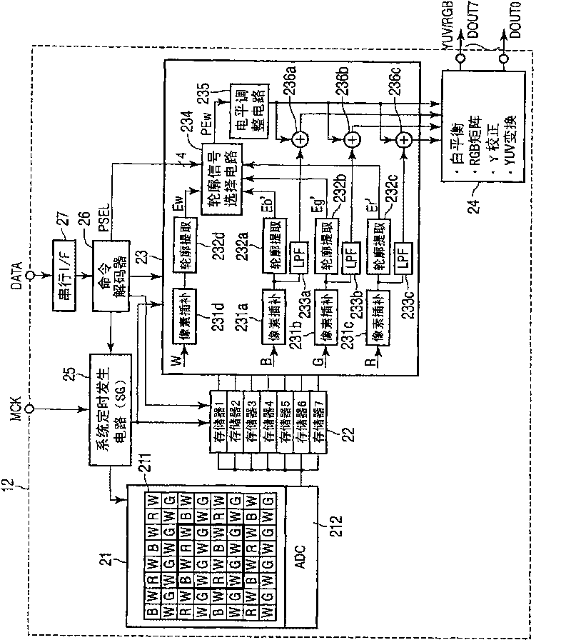
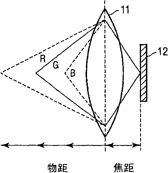
[0024] figure 1 It is a diagram showing a schematic configuration of a solid-state imaging device using the CMOS image sensor according to the first embodiment. This solid-state imaging device is constituted by a sensor chip 12, and the sensor chip 12 will pass figure 2 The optical signal condensed by the illustrated optical lens 11 is converted into an electrical signal to output a digital image signal. As will be described in detail later, as the optical lens 11 , a chromatic aberration lens having a characteristic that the focus position differs depending on the wavelength of each band of R (red), G (green), and B (blue) is used. exist figure 2 In , the focal length is represented by FD, and the object distance (distance to the object) is represented by OD.

[0025] figure 1 A circuit configuration of the sensor chip 12 included in the solid-state imaging device is shown. The sensor chip 12 includes a sensor unit 21 , a line memory 22 , a focus adjustment circuit 23 ...

no. 2 Embodiment

[0051] Figure 9 It is a block diagram showing the circuit configuration of the sensor chip 12 used in the solid-state imaging device according to the second embodiment. Also, as the optical lens 11 , a chromatic aberration lens having a characteristic that the focal position differs depending on the wavelength of each band of R (red), G (green), and B (blue) is used similarly to the first embodiment.

[0052] The difference between the sensor chip 12 in the present embodiment and the sensor chip in the first embodiment is that the color arrangement of the color filter of the sensor part 21 is in a basic 4×4 pixel arrangement, and the pixels are arranged in a grid with 8 pixels. , G pixels are arranged with 4 pixels, and R pixels are arranged with 4 pixels. By adopting such a color filter, the output of the R signal is doubled compared with the sensor chip of the first embodiment. As a result, the same high-resolution signal as that of the G pixel is obtained as the contour ...

no. 3 Embodiment

[0064] Figure 13 It is a block diagram showing the circuit configuration of the sensor chip 12 used in the solid-state imaging device according to the third embodiment. Furthermore, as the optical lens 11 , a chromatic aberration lens having the characteristic that the focal position varies with the wavelengths of the R (red), G (green), and B (blue) bands is used similarly to the first embodiment.

[0065] The difference between the sensor chip 12 in this embodiment and the sensor chip in the first embodiment is that the color arrangement of the color filters of the sensor unit 21 is arranged in a basic 2×2 pixel arrangement with two pixels arranged in G pixels and arranged in B pixels. 1 pixel, R pixel is arranged in a general Bayer arrangement of 1 pixel. As the color arrangement of such color filters is changed, a part of the focus adjustment circuit is also changed. That is, in the focus adjustment circuit 23b of this embodiment, the W signal is not input, so the pixel...


PUM


Abstract

The solid-state image pickup device includes a sensor unit and a focus adjustment circuit, the focus adjustment circuit including a contour extraction circuit which extracts contour signals from wavelength signals W, B, G, and R, a contour signal selection circuit which receives a control signal and the plurality of contour signals extracted by the contour extraction circuit, and selects and outputs a contour signal having a desired wavelength band in accordance with the control signal, and a plurality of addition circuits which add the wavelength signals before the contour signals are extracted by the contour extraction circuit to a contour signal output from a contour signal output circuit.

Description

[0001] This application is based on and claims priority from Japanese Priority Patent Application No. 2008-292237 filed on November 14, 2008, the latter application being incorporated herein by reference in its entirety. technical field [0002] The present invention relates to a solid-state imaging device incorporating a processing circuit for processing video signals such as an image sensor, which is used in a mobile phone with an image sensor, a digital camera, a video camera, and the like. Background technique [0003] With the reduction in thickness of mobile phones, there is a strong demand for miniaturization of camera modules used in mobile phones. In addition, it is required that the camera module used in a mobile phone is not easily damaged even if it is dropped. In addition, in recent years, in order to meet the demand for higher image quality, multi-pixels of 5 million pixels or 8 million pixels or more are being developed. In a multi-pixel sensor, as the pixel ...

Claims


Application Information

Patent Timeline
Patent Type & Authority Applications(China)
IPC IPC(8): H04N5/225G02B7/28G03B13/36H01L27/146H04N9/07H04N9/68
CPCH04N5/23212H04N9/045H04N2209/046H04N5/2257H04N23/959H04N23/57H04N25/611H04N25/133H04N25/135H04N23/843
Inventor 江川佳孝
Owner KK TOSHIBA
Why Eureka
Try Eureka