High voltage stabilizer and high voltage intrinsic NMOS tube

A stabilizer, high-voltage technology, applied in instruments, circuits, electrical components, etc., can solve the problems of limited driving capacity, complex manufacturing process, high cost, and achieve the effect of improving breakdown voltage, low doping concentration, and high support voltage

Active Publication Date: 2010-06-23
SHANGHAI HUAHONG GRACE SEMICON MFG CORP
View PDF0 Cites 8 Cited by
  • Summary
  • Abstract
  • Description
  • Claims
  • Application Information

AI Technical Summary

Problems solved by technology

[0002] There are usually two solutions for the high-voltage regulator circuit currently used. One is the voltage regulation circuit made of high-voltage PMOS and high-voltage NMOS. Due to the complicated manufacturing process and high cost of high-voltage PMOS and high-voltage NMOS, high-voltage PMOS and high-voltage NMOS are used. The voltage adjustment circuit will obviously increase the production cost; the other is to use a general voltage clamping circuit, such as figure 1 As shown, the external power supply VDD is connected to a clamping circuit through a current limiting resistor, and the output voltage VOUT of the voltage clamping circuit is equal to the external power supply voltage VDD minus the product of the internal circuit load current and the current limiting resistor R, so as the load current increases increase, the output voltage VOUT will decrease correspondingly, in order to meet the demand of larger load current, the current limiting resistor R can only take a smaller resistance; on the other hand, for the input of higher external power supply voltage VDD, A current-limiting resistor R with a smaller resistance value will inevitably bring greater power consumption. Therefore, common voltage clamping circuits cannot have a larger current drive capability and a smaller power consumption at the same time. The drive capability is limited and the drive capability increases. while the power consumption will increase rapidly
[0003] Existing intrinsic NMOS such as figure 2 As shown, the channel under the gate oxide layer is P-substrate silicon without ion implantation. The cost of intrinsic NMOS is low, but the gate, source and drain cannot withstand high voltage, and the threshold voltage is -0.3 Between V and 0.3V, generally only used in low-voltage circuits

Method used


Image

  • High voltage stabilizer and high voltage intrinsic NMOS tube
  • High voltage stabilizer and high voltage intrinsic NMOS tube
  • High voltage stabilizer and high voltage intrinsic NMOS tube

Examples


Embodiment Construction

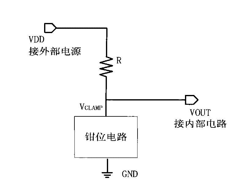
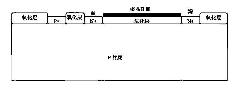
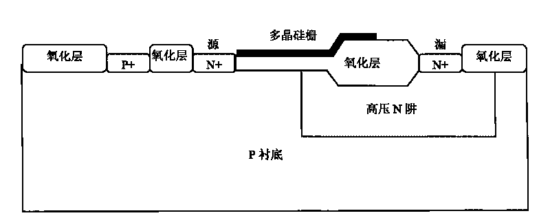
[0017] An embodiment of the high-voltage voltage stabilizer of the present invention is as follows: Figure 4 As shown, it includes a polysilicon resistor, a PMOS transistor, a first NMOS transistor, a second NMOS transistor, a PNP transistor and a high voltage intrinsic NMOS (HV Native NMOS) transistor. The external power supply end is connected to the source and substrate of the PMOS transistor through a polysilicon resistor, the gate and drain of the PMOS are connected to the gate and drain of the first NMOS, and the source of the first NMOS is connected to to the gate and drain of the second NMOS, the source of the second NMOS is connected to the emitter of the PNP, the base and the collector of the PNP are grounded, and the high voltage intrinsic The drain of the NMOS tube is connected to the external power supply terminal, the source is connected to the internal circuit as the output terminal of the high voltage voltage stabilizer, the gate is connected to the source and...


PUM


Abstract

The invention discloses a high voltage stabilizer which comprises a current limiting resistor, a clamping circuit and a high voltage intrinsic NMOS tube, wherein the current limiting resistor and the clamping circuit are connected in series between an external power source and the ground, and the source electrode of the high voltage intrinsic NMOS tube is connected with an internal circuit, the drain electrode is connected with an external electric end, and a gate electrode is connected with the current limiting resistor and the clamping circuit. The invention also discloses a high voltage intrinsic NMOS tube. A part of a gate oxide layer close to a source electrode N+ is a thin gate oxide layer; a part of the gate oxide layer close to a drain electrode N+ is a thick gate oxide layer; high voltage N wells are generated below the drain electrode N+ and the thick gate oxide layer; the high voltage N wells completely envelope the thick gate oxide layer and the drain electrode N+; the doping concentration of the high voltage N-well region is smaller than that of a P substrate region; and a polysilicon part of the gate electrode covers the thick gate oxide layer. The high voltage stabilizer of the invention has simple structure, large driving capacity and low power consumption.

Description

technical field [0001] The invention relates to semiconductor technology, in particular to a high-voltage voltage stabilizer and a high-voltage intrinsic NMOS tube. Background technique [0002] There are usually two solutions for the high-voltage regulator circuit currently used. One is the voltage regulation circuit made of high-voltage PMOS and high-voltage NMOS. Due to the complicated manufacturing process and high cost of high-voltage PMOS and high-voltage NMOS, high-voltage PMOS and high-voltage NMOS are used. The voltage adjustment circuit will obviously increase the production cost; the other is to use a general voltage clamping circuit, such as figure 1 As shown, the external power supply VDD is connected to a clamping circuit through a current limiting resistor, and the output voltage VOUT of the voltage clamping circuit is equal to the external power supply voltage VDD minus the product of the internal circuit load current and the current limiting resistor R, so a...

Claims


Application Information

Patent Timeline
Patent Type & Authority Applications(China)
IPC IPC(8): G05F3/24H01L29/78H01L29/423H01L29/06
Inventor 张宁王楠
Owner SHANGHAI HUAHONG GRACE SEMICON MFG CORP
Why Eureka
Try Eureka