Display device of built-in sensitive device
A technology of display device and display screen, which is applied in the input/output process of data processing, instruments, electronic digital data processing, etc., and can solve the problems of impractical and ineffective audio-visual entertainment systems
- Summary
- Abstract
- Description
- Claims
- Application Information
AI Technical Summary
Problems solved by technology
Method used
Image
Examples
Embodiment 1
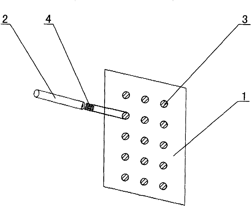
[0053] refer to figure 1 The display device with built-in induction includes a display screen 1 , a light sensing device, a monitoring device and an operating beam generating device 2 .
[0054] The photosensitive device includes a plurality of photosensitive devices 3 , and each photosensitive device 3 is arranged on the display surface of the display screen 1 . The photosensitive device 3 can sense the light incident on the photosensitive device 3 and its changes. When the photosensitive device 3 senses the change of incident light, it converts it into a change of electrical signal, that is, generates a photosensitive signal.
[0055] The operating beam generating device 2 can use a laser pointer (also can be other devices that can generate a beam), and the operating beam generating device 2 generates an operating beam 4 (such as a laser beam). When the operating beam 4 is irradiated on the position of a certain photosensitive device 3 , the light incident on the photosens...
Embodiment 2
[0076] In this embodiment, the signal of the photosensitive array is led out to the monitoring device by means of series lead-out, such as Figure 15 As shown, its characteristics are: the photosensitive array includes two sets of sub-matrixes nested with each other, the Y photosensitive sub-matrix and the X photosensitive sub-matrix, and the two sets of sub-matrices are respectively composed of a Y photosensitive device 3-1 and an X photosensitive device 3-2 (a photosensitive The device 3 corresponds to a position coordinate information, wherein the position coordinate information of the Y photosensitive device 3-1 only includes the Y-axis coordinate, and the X photosensitive device 3-2 only includes the X-axis coordinate), and configures the X-direction signal line Xn for the Y photosensitive sub-matrix (Xn1, Xn2, Xn3...), configure the Y direction signal line Ym (Ym1, Ym2, Ym3...) for the X photosensitive sub-matrix; in the Y photosensitive sub-matrix, the Y photosensitive d...
Embodiment 3
[0083] On the basis of Embodiment 1, only the structure of the photosensitive device 3 is improved, such as Figure 19 and Figure 20 As shown, the feature of the photosensitive device 3 is: an ohmic contact layer 38 is arranged between the two extraction electrodes (i.e. the first extraction electrode 32 and the second extraction electrode 33) and the silicon film, and the ohmic contact layer 38 is partially extended to the photosensitive window.
[0084] Since the extension portion 381 of the ohmic contact layer 38 has light transmittance and electrical conductivity, light can pass through the extension portion 381 and enter the photosensitive channel 34 to excite photo-induced carriers, which can move vertically to The extended portion 381 of the ohmic contact layer 38 is guided into the lead-out electrode by the conductivity of the ohmic contact layer 38 . Adopting this design scheme can increase the intensity of the photo-induced leakage current between the two electrod...
PUM
 Abstract
Description
Claims
Application Information


